PCI Express* Registers (D1:F0)
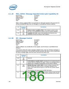
6.1.29
MSI_CAPID—Message Signaled Interrupts Capability ID
B/D/F/Type:
Address Offset:
Default Value:
Access:
0/1/0/PCI
90–91h
A005h
RO
Size:
16 bits
When a device supports MSI it can generate an interrupt request to the processor by
writing a predefined data item (a message) to a predefined memory address.
Bit
15:8
7:0
Access &
Default
Description
RO
A0h
Pointer to Next Capability (PNC): This contains a pointer to the
next item in the capabilities list which is the PCI Express capability.
RO
Capability ID (CID): Value of 05h identifies this linked list item
05h
(capability structure) as being for MSI registers.
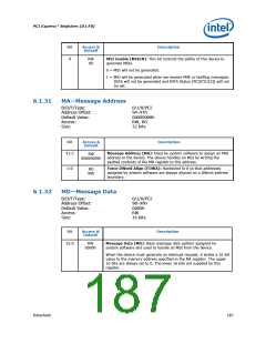
6.1.30
MC—Message Control
B/D/F/Type:
Address Offset:
Default Value:
Access:
0/1/0/PCI
92–93h
0000h
RW, RO
16 bits
Size:
System software can modify bits in this register, but the device is prohibited from
doing so.
If the device writes the same message multiple times, only one of those messages is
ensured to be serviced. If all of them must be serviced, the device must not generate
the same message again until the driver services the earlier one.
Bit
15:8
7
Access &
Default
Description
Reserved
RO
00h
64-bit Address Capable (64AC): Hardwired to 0 to indicate that the
function does not implement the upper 32 bits of the Message Address
register and is incapable of generating a 64-bit memory address.
RO
0b
6:4
RW
000b
Multiple Message Enable (MME): System software programs this
field to indicate the actual number of messages allocated to this
device. This number will be equal to or less than the number actually
requested.
The encoding is the same as for the MMC field below.
3:1
RO
Multiple Message Capable (MMC): System software reads this field
000b
to determine the number of messages being requested by this device.
000 = 1 message requested
All others are reserved.
186
Datasheet

 INTEL [ INTEL ]