DRAM Controller Registers (D0:F0)
5.2.25
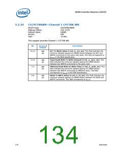
C1CYCTRKRD—Channel 1 CYCTRK READ
B/D/F/Type:
Address Offset:
Default Value:
Access:
0/0/0/MCHBAR
658–65Ah
000000h
RO, RW
24 bits
Size:
This is the Channel 1 CYCTRK READ register.
Bit
Access &
Default
Description
23:20
19:16
RO
0h
Reserved
RW
0h
Min ACT To READ Delayed (C1sd_cr_act_rd): This field indicates
the minimum allowed spacing (in DRAM clocks) between the ACT and
READ commands to the same rank-bank. This field corresponds to
tRCD_rd in the DDR Specification.
15:11
10:8
RW
00000b
Same Rank Write To READ Delayed (C1sd_cr_wrsr_rd): This
field indicates the minimum allowed spacing (in DRAM clocks)
between the WRITE and READ commands to the same rank. This field
corresponds to tWTR in the DDR Specification.
RW
0000b
Different Ranks Write To READ Delayed (C1sd_cr_wrdr_rd):
This field indicates the minimum allowed spacing (in DRAM clocks)
between the WRITE and READ commands to different ranks. This field
corresponds to tWR_RD in the DDR Specification.
7:4
3:0
RW
0000b
Same Rank Read To Read Delayed (C1sd_cr_rdsr_rd): This field
indicates the minimum allowed spacing (in DRAM clocks) between two
READ commands to the same rank.
RW
0000b
Different Ranks Read To Read Delayed (C1sd_cr_rddr_rd): This
configuration register indicates the minimum allowed spacing (in
DRAM clocks) between two READ commands to different ranks. This
field corresponds to tRD_RD
.
Datasheet
135

 INTEL [ INTEL ]