DRAM Controller Registers (D0:F0)
5.1.37
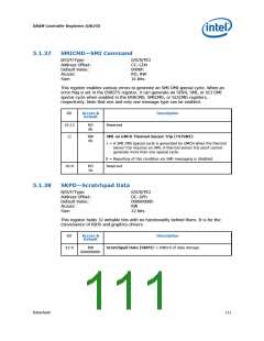
SMICMD—SMI Command
B/D/F/Type:
Address Offset:
Default Value:
Access:
0/0/0/PCI
CC–CDh
0000h
RO, RW
16 bits
Size:
This register enables various errors to generate an SMI DMI special cycle. When an
error flag is set in the ERRSTS register, it can generate an SERR, SMI, or SCI DMI
special cycle when enabled in the ERRCMD, SMICMD, or SCICMD registers,
respectively. Note that one and only one message type can be enabled.
Bit
15:12
11
Access &
Default
Description
RO
0h
Reserved
RW
0b
SMI on GMCH Thermal Sensor Trip (TSTSMI):
1 = A SMI DMI special cycle is generated by GMCH when the thermal
sensor trip requires an SMI. A thermal sensor trip point cannot
generate more than one special cycle.
0 = Reporting of this condition via SMI messaging is disabled.
Reserved
10:0
RO
0s
5.1.38
SKPD—Scratchpad Data
B/D/F/Type:
Address Offset:
Default Value:
Access:
0/0/0/PCI
DC–DFh
00000000h
RW
Size:
32 bits
This register holds 32 writable bits with no functionality behind them. It is for the
convenience of BIOS and graphics drivers.
Bit
Access &
Default
Description
31:0
RW
Scratchpad Data (SKPD): 1 DWord of data storage.
00000000h
Datasheet
111

 INTEL [ INTEL ]