DRAM Controller Registers (D0:F0)
5.1.36
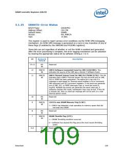
ERRCMD—Error Command
B/D/F/Type:
Address Offset:
Default Value:
Access:
0/0/0/PCI
CA–CBh
0000h
RO, RW
16 bits
Size:
This register controls the GMCH responses to various system errors. Since the GMCH
does not have an SERR# signal, SERR messages are passed from the GMCH to the
ICH over DMI.
When a bit in this register is set, a SERR message will be generated on DMI whenever
the corresponding flag is set in the ERRSTS register. The actual generation of the
SERR message is globally enabled for Device 0 via the PCI Command register.
Bit
15:13
12
Access &
Default
Description
RO
000b
Reserved
RWC/S
0b
GMCH Software Generated Event for SMI (GSGESMI): This
indicates the source of the SMI was a Device 2 Software Event.
11
RW
0b
SERR on GMCH Thermal Sensor Event (TSESERR):
1 = The GMCH generates a DMI SERR special cycle when bit 11 of the
ERRSTS is set. The SERR must not be enabled at the same time
as the SMI for the same thermal sensor event.
0 = Reporting of this condition via SERR messaging is disabled.
Reserved
10
9
RO
0b
RW
0b
SERR on LOCK to non-DRAM Memory (LCKERR):
1 = The GMCH will generate a DMI SERR special cycle whenever a
processor lock cycle is detected that does not hit DRAM.
0 = Reporting of this condition via SERR messaging is disabled.
Reserved
8:0
RW
0s
110
Datasheet

 INTEL [ INTEL ]