DRAM Controller Registers (D0:F0)
5.1.35
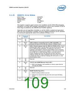
ERRSTS—Error Status
B/D/F/Type:
Address Offset:
Default Value:
Access:
0/0/0/PCI
C8–C9h
0000h
RO, RWC/S
16 bits
Size:
This register is used to report various error conditions via the SERR DMI messaging
mechanism. An SERR DMI message is generated on a zero to one transition of any of
these flags (if enabled by the ERRCMD and PCICMD registers).
These bits are set regardless of whether or not the SERR is enabled and generated.
After the error processing is complete, the error logging mechanism can be unlocked
by clearing the appropriate status bit by software writing a 1 to it.
Bit
15:13
12
Access &
Default
Description
RO
0b
Reserved
RWC/S
0b
GMCH Software Generated Event for SMI (GSGESMI): This
indicates the source of the SMI was a Device 2 Software Event.
11
RWC/S
0b
GMCH Thermal Sensor Event for SMI/SCI/SERR (GTSE): This bit
indicates that a GMCH Thermal Sensor trip has occurred and an SMI,
SCI or SERR has been generated. The status bit is set only if a
message is sent based on Thermal event enables in Error command,
SMI command and SCI command registers. A trip point can generate
one of SMI, SCI, or SERR interrupts (two or more per event is
invalid). Multiple trip points can generate the same interrupt, if
software chooses this mode, subsequent trips may be lost. If this bit
is already set, then an interrupt message will not be sent on a new
thermal sensor event.
10
9
RO
0b
Reserved
RWC/S
0b
LOCK to non-DRAM Memory Flag (LCKF):
1 = GMCH has detected a lock operation to memory space that did
not map into DRAM.
8
7
RO
0b
Reserved
RWC/S
0b
DRAM Throttle Flag (DTF):
1 = DRAM Throttling condition occurred.
0 = Software has cleared this flag since the most recent throttling
event.
6:0
RO
0s
Reserved
Datasheet
109

 INTEL [ INTEL ]