DRAM Controller Registers (D0:F0)
5.1.32
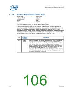
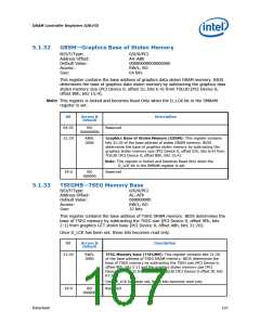
GBSM—Graphics Base of Stolen Memory
B/D/F/Type:
Address Offset:
Default Value:
Access:
0/0/0/PCI
A4–ABh
0000000000000000h
RW/L, RO
64 bits
Size:
This register contains the base address of graphics data stolen DRAM memory. BIOS
determines the base of graphics data stolen memory by subtracting the graphics data
stolen memory size (PCI Device 0, offset 52, bits 6:4) from TOLUD (PCI Device 0,
offset B0h, bits 15:4).
Note: This register is locked and becomes Read Only when the D_LCK bit in the SMRAM
register is set.
Bit
Access &
Default
Description
63:32
31:20
RO
00000000h
Reserved
RW/L
000h
Graphics Base of Stolen Memory (GBSM): This register contains
bits 31:20 of the base address of stolen DRAM memory. BIOS
determines the base of graphics stolen memory by subtracting the
graphics stolen memory size (PCI Device 0, offset 52h, bits 6:4) from
TOLUD (PCI Device 0, offset B0h, bits 15:4).
Note: This register is locked and becomes Read Only when the
D_LCK bit in the SMRAM register is set.
19:0
RO
Reserved
00000h
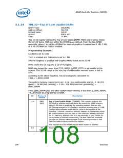
5.1.33
TSEGMB—TSEG Memory Base
B/D/F/Type:
Address Offset:
Default Value:
Access:
0/0/0/PCI
AC–AFh
00000000h
RW/L, RO
32 bits
Size:
This register contains the base address of TSEG DRAM memory. BIOS determines the
base of TSEG memory by subtracting the TSEG size (PCI Device 0, offset 9Eh, bits
2:1) from graphics GTT stolen base (PCI Device 0, offset A8h, bits 31:20).
Once D_LCK has been set, these bits becomes read only.
Bit
Access &
Default
Description
31:20
RW/L
000h
TESG Memory base (TSEGMB): This register contains bits 31:20
of the base address of TSEG DRAM memory. BIOS determines the
base of TSEG memory by subtracting the TSEG size (PCI Device 0,
offset 9Eh, bits 2:1) and the graphics stolen memory size (PCI
Device 0 offset 52 bits 6:4) from TOLUD (PCI Device 0 offset 9C bits
07:02).
Once D_LCK has been set, these bits becomes read only.
Reserved
19:0
RO
00000h
Datasheet
107

 INTEL [ INTEL ]