DRAM Controller Registers (D0:F0)
Bit
Access &
Default
Description
0
RW/L
0b
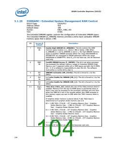
TSEG Enable (T_EN): Enabling of SMRAM memory for Extended
SMRAM space only. When G_SMRAME = 1 and TSEG_EN = 1, the TSEG
is enabled to appear in the appropriate physical address space. Note
that once D_LCK is set, this bit becomes read only.
5.1.30
TOM—Top of Memory
B/D/F/Type:
Address Offset:
Default Value:
Access:
0/0/0/PCI
A0–A1h
0001h
RO, RW/L
16 bits
Size:
This Register contains the size of physical memory. BIOS determines the memory size
reported to the OS using this Register.
Bit
15:10
9:0
Access &
Default
Description
RO
00h
Reserved
RW/L
001h
Top of Memory (TOM): This register reflects the total amount of
populated physical memory. This is NOT necessarily the highest main
memory address (holes may exist in main memory address map due
to addresses allocated for memory mapped I/O). These bits
correspond to address bits 35:26 (64 MB granularity). Bits 25:0 are
assumed to be 0.
Datasheet
105

 INTEL [ INTEL ]