DRAM Controller Registers (D0:F0)
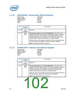
5.1.26
REMAPBASE—Remap Base Address Register
B/D/F/Type:
Address Offset:
Default Value:
Access:
0/0/0/PCI
98–99h
03FFh
RO, RW
16 bits
Size:
Bit
15:10
9:0
Access &
Description
Default
RO
000000b
Reserved
RW/L
3FFh
Remap Base Address [35:26] (REMAPBASE): The value in this
register defines the lower boundary of the Remap window. The Remap
window is inclusive of this address. In the decoder A[25:0] of the
Remap Base Address are assumed to be 0s. Thus, the bottom of the
defined memory range will be aligned to a 64 MB boundary.
When the value in this register is greater than the value programmed
into the Remap Limit register, the Remap window is disabled.
Note: Bit 0 (Address Bit 26) must be a 0.
5.1.27
REMAPLIMIT—Remap Limit Address Register
B/D/F/Type:
Address Offset:
Default Value:
Access:
0/0/0/PCI
9A–9Bh
0000h
RO, RW
16 bits
Size:
Bit
15:10
9:0
Access &
Description
Default
RO
000000b
Reserved
RW/L
000h
Remap Limit Address [35:26] (REMAPLMT): The value in this
register defines the upper boundary of the Remap window. The Remap
window is inclusive of this address. In the decoder A[25:0] of the
remap limit address are assumed to be Fhs. Thus the top of the
defined range will be one less than a 64 MB boundary.
When the value in this register is less than the value programmed into
the Remap Base register, the Remap window is disabled.
Note: Bit 0 (Address Bit 26) must be a 0.
102
Datasheet

 INTEL [ INTEL ]