DRAM Controller Registers (D0:F0)
5.1.25
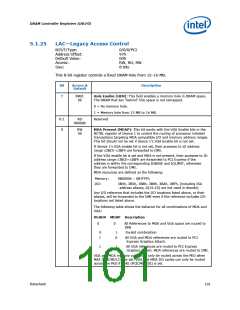
LAC—Legacy Access Control
B/D/F/Type:
Address Offset:
Default Value:
Access:
0/0/0/PCI
97h
00h
RW, RO, RW
8 bits
Size:
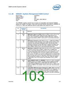
This 8-bit register controls a fixed DRAM hole from 15–16 MB.
Bit
Access &
Default
Description
7
RW/L
0b
Hole Enable (HEN): This field enables a memory hole in DRAM space.
The DRAM that lies "behind" this space is not remapped.
0 = No memory hole.
1 = Memory hole from 15 MB to 16 MB.
Reserved
6:1
0
RO
00000b
RW
0b
MDA Present (MDAP): This bit works with the VGA Enable bits in the
BCTRL register of Device 1 to control the routing of processor initiated
transactions targeting MDA compatible I/O and memory address ranges.
This bit should not be set if device 1's VGA Enable bit is not set.
If device 1's VGA enable bit is not set, then accesses to IO address
range x3BCh–x3BFh are forwarded to DMI.
If the VGA enable bit is set and MDA is not present, then accesses to IO
address range x3BCh–x3BFh are forwarded to PCI Express if the
address is within the corresponding IOBASE and IOLIMIT, otherwise
they are forwarded to DMI.
MDA resources are defined as the following:
Memory:
I/O:
0B0000h – 0B7FFFh
3B4h, 3B5h, 3B8h, 3B9h, 3BAh, 3BFh, (including ISA
address aliases, A[15:10] are not used in decode)
Any I/O reference that includes the I/O locations listed above, or their
aliases, will be forwarded to the DMI even if the reference includes I/O
locations not listed above.
The following table shows the behavior for all combinations of MDA and
VGA:
VGAEN MDAP Description
0
0
All References to MDA and VGA space are routed to
DMI
0
1
Invalid combination
1
0
All VGA and MDA references are routed to PCI
Express Graphics Attach.
1
1
All VGA references are routed to PCI Express
Graphics Attach. MDA references are routed to DMI.
VGA and MDA memory cycles can only be routed across the PEG when
MAE (PCICMD1[1]) is set. VGA and MDA I/O cycles can only be routed
across the PEG if IOAE (PCICMD1[0]) is set.
Datasheet
101

 INTEL [ INTEL ]