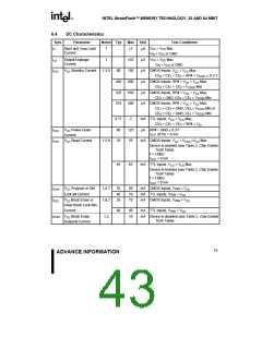
INTEL StrataFlash™ MEMORY TECHNOLOGY, 32 AND 64 MBIT
E
Min
120
150
(1)
6.5
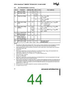
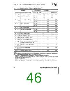
AC Characteristics— Read-Only Operations
Versions
5 V ± 10% VCCQ
2.7 V—3.6V VCCQ
Notes
–120/–150(4)
(All units in ns unless otherwise noted)
–L120/–L150(4)
#
Sym
Parameter
Min
120
150
Max
Max
R1 tAVAV Read/Write Cycle Time
R2 tAVQV Address to Output Delay
R3 tELQV CEX to Output Delay
32 Mbit
64 Mbit
32 Mbit
120
150
120
150
50
120
150
120
150
50
64 Mbit
32 Mbit
64 Mbit
2
2
2
R4 tGLQV OE# to Output Delay
R5 tPHQV RP# High to Output Delay
32 Mbit
64 Mbit
180
210
180
210
R6 tELQX CEX to Output in Low Z
R7 tGLQX OE# to Output in Low Z
R8 tEHQZ CEX High to Output in High Z
R9 tGHQZ OE# High to Output in High Z
3
3
3
3
3
0
0
0
0
55
15
55
15
R10 tOH
Output Hold from Address, CEX, or OE#
Change, Whichever Occurs First
0
0
R11 tELFL CEX Low to BYTE# High or Low
tELFH
3
10
10
R12 tFLQV BYTE# to Output Delay
tFHQV
1000
1000
1000
1000
R13 tFLQZ BYTE# to Output in High Z
3
NOTES:
CEX low is defined as the first edge of CE , CE , or CE that enables the device. CEX high is defined at the first edge of CE ,
0
1
2
0
CE , or CE that disables the device (see Table 2, Chip Enable Truth Table).
1
2
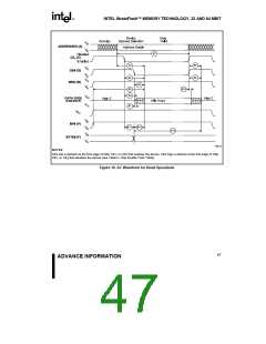
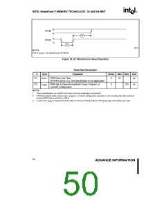
1. See Figure 16, AC Waveform for Read Operations for the maximum allowable input slew rate.
2. OE# may be delayed up to tELQV-tGLQV after the first edge of CE , CE , or CE that enables the device (see Table 2, Chip
0
1
2
Enable Truth Table) without impact on tELQV
.
3. Sampled, not 100% tested.
4. See Figures 13–15, Transient Input/Output Reference Waveform for VCCQ = 5.0 V ±10%, Transient Input/Output
Reference Waveform for VCCQ = 2.7 V –3.6 V, and Transient Equivalent Testing Load Circuit for testing characteristics.
46
ADVANCE INFORMATION

 INTEL [ INTEL ]