INTEL StrataFlash™ MEMORY TECHNOLOGY, 32 AND 64 MBIT
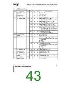
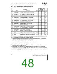
6.4 DC Characteristics (Continued)
E
Sym
Parameter
Input Low Voltage
Input High Voltage
Notes Min
Max
Unit
V
Test Conditions
VIL
7
–0.5
2.0
0.8
VIH
7
VCC
+ 0.5
0.45
V
VOL
Output Low Voltage
3,7
V
V
V
VCCQ = VCCQ1 Min
IOL = 5.8 mA
0.4
VCCQ = VCCQ2 Min
IOL = 2 mA
3,7
3,7
2.4
VOH1 Output High Voltage
(TTL)
V
CCQ = VCCQ1 Min or VCCQ = VCCQ2 Min
IOH = –2.5 mA (VCCQ1
–2 mA (VCCQ2
CCQ = VCCQ1 Min or VCCQ = VCCQ2 Min
)
)
0.85
V
V
V
V
VOH2 Output High Voltage
(CMOS)
V
VCCQ
IOH = –2.5 mA
VCCQ
–0.4
VCCQ = VCCQ1 Min or VCCQ = VCCQ2 Min
IOH = –100 µA
4,7,11 3.6
VPENLK VPEN Lockout during
Normal Operations
4,11
VPENH VPEN during Block
Erase, Program, or
4.5
5.5
Lock-Bit Operations
8
3.25
11.4
V
V
VLKO VCC Lockout Voltage
9,10
12.6
Set master lock-bit
Override lock-bit
VHH
RP# Unlock Voltage
NOTES:
1.
All currents are in RMS unless otherwise noted. These currents are valid for all product versions (packages and speeds).
Contact Intel’s Application Support Hotline or your local sales office for information about typical specifications.
2.
ICCES is specified with the device de-selected. If the device is read or written while in erase suspend mode, the device’s
current draw is ICCR or ICCW
.
3.
4.
Includes STS.
Block erases, programming, and lock-bit configurations are inhibited when VPEN ≤ VPENLK, and not guaranteed in the
range between VPENLK (max) and VPENH (min), and above VPENH (max).
5.
6.
7.
8.
CMOS inputs are either VCC ± 0.2 V or GND ± 0.2 V. TTL inputs are either VIL or VIH
Add 5 mA for VCCQ = VCCQ2 min.
.
Sampled, not 100% tested.
Block erases, programming, and lock-bit configurations are inhibited when VCC < VLKO, and not guaranteed in the range
between VLKO (max) and VCC (min), and above VCC (max).
9.
Master lock-bit set operations are inhibited when RP# = V . Block lock-bit configuration operations are inhibited when the
IH
master lock-bit is set and RP# = VIH. Block erases and programming are inhibited when the corresponding block-lock bit
is set and RP# = VIH. Block erase, program, and lock-bit configuration operations are not guaranteed and should not be
attempted with VIH < RP# < VHH
.
10. RP# connection to a VHH supply is allowed for a maximum cumulative period of 80 hours.
11. Tie VPEN to VCC (4.5 V–5.5 V).
44
ADVANCE INFORMATION

 INTEL [ INTEL ]