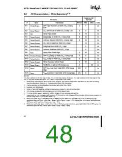
INTEL StrataFlash™ MEMORY TECHNOLOGY, 32 AND 64 MBIT
E
Unit
(1,2)
6.6
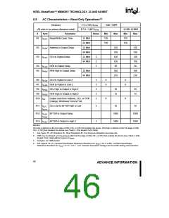
AC Characteristics— Write Operations
Valid for All
Speeds
Versions
#
Sym
tPHWL ( PHEL)
Parameter
Notes
Min
Max
W1
t
RP# High Recovery to WE# (CEX ) Going
Low
3
1
µs
W2
W3
W4
W5
W6
W7
W8
W9
tELWL (tWLEL
tWP
tDVWH ( DVEH)
tAVWH ( AVEH)
tWHEH ( EHWH)
tWHDX ( EHDX)
tWHAX ( EHAX)
tWPH
)
CEX (WE#) Low to WE# (CEX) Going Low
Write Pulse Width
8
8
4
4
0
70
50
50
10
0
ns
ns
ns
ns
ns
ns
ns
ns
ns
ns
ns
ns
ns
t
Data Setup to WE# (CEX ) Going High
Address Setup to WE# (CEX ) Going High
CEX (WE#) Hold from WE# (CEX) High
Data Hold from WE# (CEX ) High
Address Hold from WE# (CEX ) High
Write Pulse Width High
t
t
t
t
0
9
30
0
W10 tPHHWH ( PHHEH)
W11 tVPWH ( VPEH)
W12 tWHGL ( EHGL)
W13 tWHRL ( EHRL)
t
RP# VHH Setup to WE# (CEX ) Going High
VPEN Setup to WE# (CEX ) Going High
Write Recovery before Read
3
3
t
0
t
6
35
t
WE# (CEX ) High to STS Going Low
5
90
W14 tQVPH
RP# VHH Hold from Valid SRD, STS Going
High
3,5,7
0
0
W15 tQVVL
VPEN Hold from Valid SRD, STS Going High
3,5,7
ns
NOTES:
CEX low is defined as the first edge of CE , CE , or CE that enables the device. CEX high is defined at the first edge of CE ,
0
1
2
0
CE , or CE that disables the device (see Table 2, Chip Enable Truth Table).
1
2
1. Read timing characteristics during block erase, program, and lock-bit configuration operations are the same as during
read-only operations. Refer to AC Characteristics–Read-Only Operations.
2. A write operation can be initiated and terminated with either CEX or WE#.
3. Sampled, not 100% tested.
4. Refer to Table 4 for valid AIN and DIN for block erase, program, or lock-bit configuration.
5. STS timings are based on STS configured in its RY/BY# default mode.
6. For array access, tAVQV is required in addition to tWHGL for any accesses after a write.
7.
V
PEN should be held at VPENH (and if necessary RP# should be held at VHH) until determination of block erase, program, or
lock-bit configuration success (SR.1/3/4/5 = 0).
8. Write pulse width (tWP) is defined from CEX or WE# going low (whichever goes low first) to CEX or WE# going high
(whichever goes high first). Hence, tWP = tWLWH = tELEH = tWLEH = tELWH. If CEX is driven low 10 ns before WE# going low,
WE# pulse width requirement decreases to tWP - 10 ns.
9. Write pulse width high (tWPH) is defined from CEX or WE# going high (whichever goes high first) to CEX or WE# going low
(whichever goes low first). Hence, tWPH = tWHWL = tEHEL = tWHEL = tEHWL
.
48
ADVANCE INFORMATION

 INTEL [ INTEL ]