INTEL StrataFlash™ MEMORY TECHNOLOGY, 32 AND 64 MBIT
E
6.0 ELECTRICAL SPECIFICATIONS
NOTICE: This datasheet contains information on products
in the sampling and initial production phases of
development. The specifications are subject to change
without notice. Verify with your local Intel Sales office that
you have the latest datasheet before finalizing a design.
6.1
Absolute Maximum Ratings*
Commercial Operating Temperature
During Read, Block Erase, Program,
*WARNING: Stressing the device beyond the “Absolute
Maximum Ratings” may cause permanent damage. These
are stress ratings only. Operation beyond the “Operating
Conditions” is not recommended and extended exposure
beyond the “Operating Conditions” may affect device
reliability.
and Lock-Bit Configuration .....0 °C to +70 °C(1)
Temperature under Bias........ –10 °C to +80 °C
Storage Temperature................. –65 °C to +125 °C
Voltage On Any Pin (except RP#)
............................................ –2.0 V to +7.0 V(2)
RP# Voltage with Respect to
GND during Lock-Bit
Configuration Operations–2.0 V to +14.0 V(2,3,4)
Output Short Circuit Current.....................100 mA(5)
NOTES:
1. Operating temperature is for commercial product defined by this specification.
2. All specified voltages are with respect to GND. Minimum DC voltage is –0.5 V on input/output pins and –0.2 V on VCC and
V
PEN pins. During transitions, this level may undershoot to–2.0 V for periods <20 ns. Maximum DC voltage on input/output
pins, VCC, and VPEN is VCC +0.5 V which, during transitions, may overshoot to VCC +2.0 V for periods <20 ns.
3. Maximum DC voltage on RP# may overshoot to +14.0 V for periods <20 ns.
4. RP# voltage is normally at VIL or VIH. Connection to supply of VHH is allowed for a maximum cumulative period of 80 hours.
5. Output shorted for no more than one second. No more than one output shorted at a time.
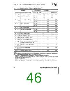
6.2
Operating Conditions
Temperature and VCC Operating Conditions
Symbol
Parameter
Notes Min
Max
+70
Unit
°C
V
Test Condition
TA
Operating Temperature
0
Ambient Temperature
VCC
VCC1 Supply Voltage (5 V ± 10%)
VCCQ1 Supply Voltage (5 V ± 10%)
VCCQ2 Supply Voltage (2. 7V−3.6 V)
4.50
4.50
2.70
5.50
5.50
3.60
VCCQ1
VCCQ2
V
V
(1)
6.3
Capacitance
TA = +25 °C, f = 1 MHz
Symbol
Parameter
Typ
6
Max
Unit
Condition
VIN = 0.0 V
VOUT = 0.0 V
CIN
Input Capacitance
Output Capacitance
8
pF
pF
COUT
NOTE:
8
12
1. Sampled, not 100% tested.
42
ADVANCE INFORMATION

 INTEL [ INTEL ]