E
INTEL StrataFlash™ MEMORY TECHNOLOGY, 32 AND 64 MBIT
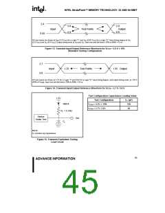
2.4
2.0
0.8
2.0
Output
0.8
Input
Test Points
0.45
AC test inputs are driven at VOH (2.4 VTTL) for a Logic "1" and VOL (0.45 VTTL) for a Logic "0." Input timing begins at V
IH
(2.0 VTTL) and VIL (0.8 VTTL). Output timing ends at VIH and VIL. Input rise and fall times (10% to 90%) <10 ns.
Figure 13. Transient Input/Output Reference Waveform for VCCQ = 5.0 V ± 10%
(Standard Testing Configuration)
2.7
Input
1.35
Test Points
1.35 Output
0.0
AC test inputs are driven at 2.7V for a Logic "1" and 0.0V for a Logic "0." Input timing begins, and output timing ends, at 1.35 V
(50% of VCCQ). Input rise and fall times (10% to 90%) <10 ns.
Figure 14. Transient Input/Output Reference Waveform for VCCQ = 2.7 V−3.6 V
Test Configuration Capacitance Loading Value
1.3V
Test Configuration
VCCQ = 5.0V ± 10%
VCCQ = 2.7V−3.6V
CL (pF)
100
1N914
50
RL = 3.3 k
Ω
Device
Under Test
Out
CL
NOTE:
CL Includes Jig Capacitance
Figure 15. Transient Equivalent Testing
Load Circuit
45
ADVANCE INFORMATION

 INTEL [ INTEL ]