E
INTEL StrataFlash™ MEMORY TECHNOLOGY, 32 AND 64 MBIT
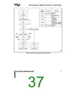
The CUI latches commands issued by system
software and is not altered by VPEN, CE0, CE1, or
CE2 transitions, or WSM actions. Its state is read
array mode upon power-up, after exit from
reset/power-down mode, or after VCC transitions
below VLKO. VCC must be kept at or above VPEN
during VCC transitions.
A system designer must guard against spurious
writes for VCC voltages above VLKO when VPEN is
active. Since WE# must be low and the device
enabled (see Table 2, Chip Enable Truth Table) for
a command write, driving WE# to VIH or disabling
the device will inhibit writes. The CUI’s two-step
command sequence architecture provides added
protection against data alteration.
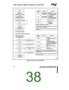
After block erase, program, or lock-bit configuration,
even after VPEN transitions down to VPENLK, the CUI
must be placed in read array mode via the Read
Array command if subsequent access to the
memory array is desired. VPEN must be kept at or
below VCC during VPEN transitions.
Keeping VPEN below VPENLK prevents inadvertent
data alteration. In-system block lock and unlock
capability protects the device against inadvertent
programming. The device is disabled while RP# =
V
IL regardless of its control inputs.
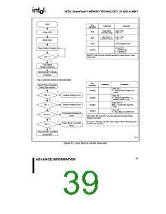
5.5
Power-Up/Down Protection
5.6
Power Dissipation
The device is designed to offer protection against
accidental block erasure, programming, or lock-bit
configuration during power transitions. Internal
circuitry resets the CUI to read array mode at
power-up.
When designing portable systems, designers must
consider battery power consumption not only during
device operation, but also for data retention during
system idle time. Flash memory’s nonvolatility
increases usable battery life because data is
retained when system power is removed.
41
ADVANCE INFORMATION

 INTEL [ INTEL ]