INTEL StrataFlash™ MEMORY TECHNOLOGY, 32 AND 64 MBIT
E
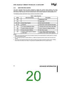
4.2.1 QUERY STRUCTURE OUTPUT
4.1
Read Array Command
The Query “database,” described later, allows
system software to gain critical information for
controlling the flash component. This section
describes the device’s CFI-compliant interface that
allows the host system to access Query data.
Upon initial device power-up and after exit from
reset/power-down mode, the device defaults to read
array mode. This operation is also initiated by
writing the Read Array command. The device
remains enabled for reads until another command
is written. Once the internal WSM has started a
block erase, program, or lock-bit configuration, the
device will not recognize the Read Array command
until the WSM completes its operation unless the
WSM is suspended via an Erase Suspend
command. The Read Array command functions
independently of the VPEN voltage and RP# can be
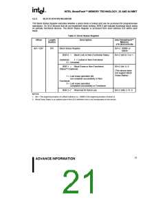
Query data are always presented on the lowest-
order data outputs DQ0–DQ7 only. The Query table
device starting address is a 10h word address.
The first two bytes of the Query structure, “Q” and
”R” in ASCII, appear on the low byte at word
addresses 10h and 11h. This CFI-compliant device
outputs 00H data on upper bytes. Thus, the device
outputs ASCII “Q” in the low byte DQ0–DQ7 and
V
IH or VHH
.
00h in the high byte DQ8–DQ15
.
4.2
Read Query Mode Command
Since the device is x8/x16 capable, the x8 data is
still presented in word-relative (16-bit) addresses.
However, the “fill data” (00h) is not the same as
driven by the upper bytes in the x16 mode. As in
x16 mode, the byte address (A0 or A1 depending on
pinout) is ignored for Query output so that the “odd
byte address” (A0 or A1 high) repeats the “even byte
address” data (A0 or A1 low). Therefore, in x8 mode
using byte addressing, the device will output the
sequence “Q,” “Q,” “R,” “R,” “Y,” “Y,” and so on,
beginning at byte-relative address 20h (which is
equivalent to word offset 10h in x16 mode).
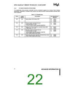
This section defines the data structure or
“database” returned by the SCS (Scaleable
Command Set) Query command. System software
should parse this structure to gain critical
information to enable programming, block erases,
and otherwise control the flash component. The
SCS Query is part of an overall specification for
multiple command set and control interface
descriptions called Common Flash Interface, or
CFI. The Query can only be accessed when the
WSM is off or the device is suspended.
In Query addresses where two or more bytes of
information are located, the least significant data
byte is presented on the lower address, and the
most significant data byte is presented on the
higher address.
18
ADVANCE INFORMATION

 INTEL [ INTEL ]