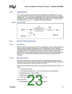
Ultra-Low Voltage Intel® Celeron® Processor — 650 MHz and 400 MHz
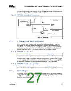
Figure 4 shows the system level connections for the VTTPWRGD signal. Refer to the appropriate
VR and system level guidelines provided by Intel for more details.
Figure 4. VTTPWRGD System-Level Connections
Vcct
Vcct
Processor
Voltage Regulator
1k
Vcct
Vttpwrgd
(output)
Vttpwrgd
(input)
3.3V
100k
10k
Clock Generator
Vttpwrgd#
(input)
1.2V to 3.3V Level Shifter
3.2.5
VTTPWRGD Signal Quality Specification
The VTTPWRGD signal is an input to the processor used to determine that the VTT power is
stable and the VID and BSEL signals should be driven to their final state by the processor. To
ensure the processor correctly reads this signal, it must meet the following requirement while the
signal is in its transition region of 300 mV to 900 mV. Also, VTTPWRGD should only enter the
transition region once, after VTT is at nominal values, for the assertion of the signal.
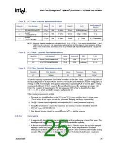
Table 11. VTTPWRGD Noise Specification
Parameter
Specification
Amount of noise (glitch)
Less than 100 mV
In addition, the VTTPWRGD signal should have reasonable transition time through the transition
region. A sharp edge on the signal transition will minimize the chance of noise causing a glitch on
this signal. Intel recommends the following transition time for the VTTPWRGD signal.
Table 12. VTTPWRGD Transition Time Specification
Parameter
Recommendation
Transition time (300 mV to 900 mV)
Less than or equal to 100 µs
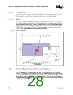
3.2.5.1
Transition Region
The transition region covered by this requirement is 300 mV to 900 mV. Once the VTTPWRGD
signal is in that voltage range, the processor is more sensitive to noise, which may be present on the
signal. The transition region when the signal first crosses the 300 mV voltage level and continues
until the last time it is below 900 mV.
Datasheet
27

 INTEL [ INTEL ]