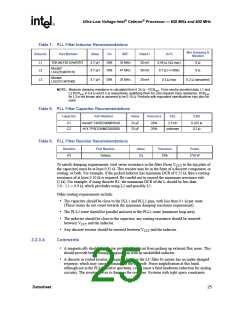
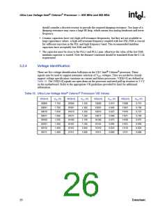
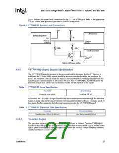
Ultra-Low Voltage Intel® Celeron® Processor — 650 MHz and 400 MHz
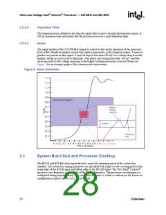
Multiplying the bus clock frequency is necessary to increase performance while allowing for easier
distribution of signals within the system. Clock multiplication within the processor is provided by
the internal Phase Lock Loop (PLL), which requires constant frequency BCLK and BCLK# inputs.
During Reset or on exit from the Deep Sleep state, the PLL requires some amount of time to
acquire the phase of BCLK and BCLK#. This time is called the PLL lock latency, which is
specified in Section 3.6, AC timing parameters T18 and T47.
3.4
Maximum Ratings
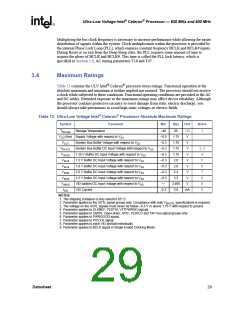
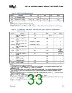
Table 13 contains the ULV Intel® Celeron® processor stress ratings. Functional operation at the
absolute maximum and minimum is neither implied nor ensured. The processor should not receive
a clock while subjected to these conditions. Functional operating conditions are provided in the AC
and DC tables. Extended exposure to the maximum ratings may affect device reliability. Although
the processor contains protective circuitry to resist damage from static electric discharge, you
should always take precautions to avoid high static voltages or electric fields.
Table 13. Ultra-Low Voltage Intel® Celeron® Processor Absolute Maximum Ratings
Symbol
Parameter
Min
Max
Unit
Notes
TStorage
Storage Temperature
–40
–0.5
–0.3
–0.3
–0.3
–0.3
–0.3
–0.3
–0.3
—
85
1.75
1.75
1.75
1.75
2.0
° C
V
1
VCC(Abs) Supply Voltage with respect to VSS
VCCT
VIN GTL
VIN125
VIN15
System Bus Buffer Voltage with respect to VSS
V
System Bus Buffer DC Input Voltage with respect to VSS
1.25 V Buffer DC Input Voltage with respect to VSS
1.5 V Buffer DC Input Voltage with respect to VSS
1.8 V Buffer DC Input Voltage with respect to VSS
2.0 V Buffer DC Input Voltage with respect to VSS
2.5 V Buffer DC Input Voltage with respect to VSS
VID ball/pin DC Input Voltage with respect to VSS
VID Current
V
2, 3
4
V
V
5
VIN18
2.0
V
6
VIN20
2.4
V
7
VIN25
3.3
V
9
VINVID
IVID
3.465
3.6
V
8
-0.3
mA
8
NOTES:
1. The shipping container is only rated for 65° C.
2. Parameter applies to the AGTL signal groups only. Compliance with both V
specifications is required.
IN GTL
3. The voltage on the AGTL signals must never be below –0.3 V or above 1.75 V with respect to ground.
4. Parameter applies to CLKREF, TESTHI, VTTPWRGD signals.
5. Parameter applies to CMOS, Open-drain, APIC, TESTLO and TAP bus signal groups only.
6. Parameter applies to PWRGOOD signal.
7. Parameter applies to PICCLK signal.
8. Parameter applies to each VID pin/ball individually.
9. Parameter applies to BCLK signal in Single Ended Clocking Mode.
Datasheet
29

 INTEL [ INTEL ]