Ultra-Low Voltage Intel® Celeron® Processor — 650 MHz and 400 MHz
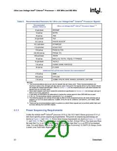
Table 6. Recommended Resistors for Ultra-Low Voltage Intel® Celeron® Processor Signals
Recommended
Resistor Value (Ω)
Ultra-Low Voltage Intel® Celeron® Processor Signal 1, 2
10 pull-down
14 pull-up
BREQ0#3
NCTRL
39 pull-up
TMS
39 pull-down
56.2 pull-up
56.2 pull-down
110 pull-down
150 pull-up
TCK
PRDY#, RESET#4
RTTIMPEDP
EDGECTRLP
PICD[1:0], TDO
PREQ#, TDI
200-300 pull-up
500 pull-down
1K pull-up
TRST#
BSEL[1:0], TESTHI, VID[4:0], VTTPWRGD
TESTLO
1K pull-down
1.5k pull-up
3K pull-up
FERR#, IERR#, PWRGOOD
FLUSH#
Additional Pull-up/Pull-down Resistor Recommendations6
270 pull-up
680 pull-up
1.5k pull-up
SMI#
STPCLK#
A20M#, DPSLP#, INIT#, IGNNE#, LINT0/INTR, LINT1/NMI
NOTES:
1. The recommendations above are only for signals that are being used. These recommendations are
maximum values only; stronger pull-ups may be used. Pull-ups for the signals driven by the chipset should
not violate the chipset specification. Refer to Section 3.1.4 for the required pull-up or pull-down resistors for
signals that are not being used.
2. Open-drain signals must never violate the undershoot specification in Section 4.3. Use stronger pull-ups if
there is too much undershoot.
3. A pull-down on BREQ0# is an alternative to having the central agent to drive BREQ0# low at reset.
4. A 56.2 Ω 1% terminating resistor connected to VCCT is required.
5. The following signals are actively driven high by the ICH3-M component and do not need external pull up
resistors on ICH3-M based platforms: A20M#, DPSLP#, INIT#, IGNNE#, LINT0/INTR, LINT1/NMI, SMI#,
STPCLK#.
6. These pull up recommendations apply to systems on which these signals are not actively pulled high such
as those utilizing the 82443MX chipset.
3.1.1
Power Sequencing Requirements
Unlike the Mobile Intel® Celeron® processor (0.18 µ), the ULV Intel Celeron processor (0.13 µ)
does have specific power sequencing requirements. The power on sequencing and timings are
shown in Figure 12 and Table 26. Power down timing requirements are shown in Figure 13, Figure
14, and Table 26. The V power plane must not rise too fast. At least 200 µs (T ) must pass from
CC
R
the time that V is at 10% of its nominal value until the time that V is at 90% of its nominal
CC
CC
value. For more details, refer to the Intel® Mobile Voltage Positioning -II (IMVP-II) Design Guide
(contact your Field Sales Representative).
20
Datasheet

 INTEL [ INTEL ]