Ultra-Low Voltage Intel® Celeron® Processor — 650 MHz and 400 MHz
3.0
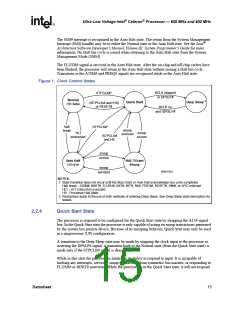
Electrical Specifications
3.1
Processor System Signals
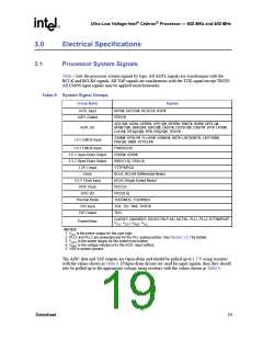
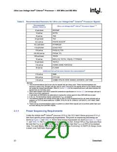
Table 5 lists the processor system signals by type. All AGTL signals are synchronous with the
BCLK and BCLK# signals. All TAP signals are synchronous with the TCK signal except TRST#.
All CMOS input signals may be applied asynchronously.
Table 5. System Signal Groups
Group Name
Signals
AGTL Input
BPRI#, DEFER#, RESET#, RSP#
PRDY#
AGTL Output
A[35:3]#, ADS#, AERR#, AP[1:0]#, BERR#, BINIT#, BNR#, BP[3:2]#,
BPM[1:0]#, BREQ0#, D[63:0]#, DBSY#, DEP[7:0]#, DRDY#, HIT#, HITM#,
LOCK#, REQ[4:0]#, RP#, RS[2:0]#, TRDY#
AGTL I/O
A20M#, DPSLP#, FLUSH#, IGNNE#, INIT#, LINT0/INTR, LINT1/NMI,
PREQ#, SMI#, STPCLK#
1.5 V CMOS Input
1.8 V CMOS Input
1.5 V Open Drain Output
3.3 V Open Drain Output
1.25 V input
PWRGOOD
FERR#, IERR#
BSEL[1:0], VID[4:0]
VTTPWRGD
Clock
BCLK, BCLK# (Differential Mode)
BCLK (Single Ended Mode)
PICCLK
2.5 V Clock Input
APIC Clock
APIC I/O
PICD[1:0]
Thermal Diode
TAP Input
THERMDC, THERMDA
TCK, TDI, TMS, TRST#
TDO
TAP Output
CLKREF, CMOSREF, EDGECTRLP, NC, NCTRL, PLL1, PLL2, RTTIMPEDP,
VCC, VCCT, VREF, VSS,
Power/Other
NOTES:
1. VCC is the power supply for the core logic.
2. PLL1 and PLL2 are power/ground for the PLL analog section. See Section 3.2.2 for details.
3. VCCT is the power supply for the system bus buffers.
4. VREF is the voltage reference for the AGTL input buffers.
5. VSS is system ground.
The APIC data and TAP outputs are Open-drain and should be pulled up to 1.5 V using resistors
with the values shown in Table 6. If Open-drain drivers are used for input signals, then they should
also be pulled up to the appropriate voltage using resistors with the values shown in Table 6.
Datasheet
19

 INTEL [ INTEL ]