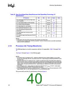
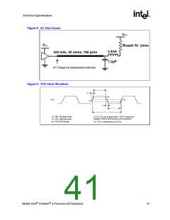
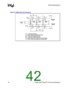
Electrical Specifications
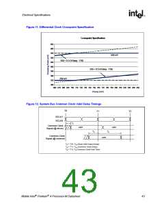
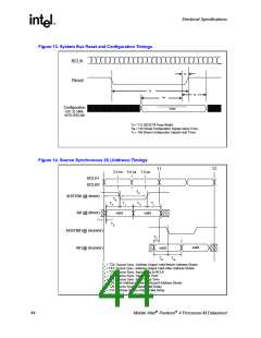
Figure 13. System Bus Reset and Configuration Timings
BCLK
Tt
Reset
Tv
Tx
Tw
Configuration
A[31:3], SMI#,
INIT#, BR[3:0]#
Valid
Tv = T13 (RESET# Pulse Width)
Tw = T45 (Reset Configuration Signals Setup TIme)
Tx = T46 (Reset Configuration Signals Hold TIme)
Figure 14. Source Synchronous 2X (Address) Timings
T1
T2
2.5 ns 5.0 ns 7.5 ns
BCLK1
BCLK0
TP
ADSTB# (@ driver)
A# (@ driver)
TR
TH
TJ
TH
TJ
valid
valid
TS
ADSTB# (@ receiver)
A# (@ receiver)
TK
valid
valid
TN
TM
TH = T23: Source Sync. Address Output Valid Before Address Strobe
TJ = T24: Source Sync. Address Output Valid After Address Strobe
TK = T27: Source Sync. Input Setup to BCLK
T
T
T
T
T
M = T26: Source Sync. Input Hold Time
N = T25: Source Sync. Input Setup Time
P = T28: First Address Strobe to Second Address Strobe
S = T20: Source Sync. Output Valid Delay
R = T31: Address Strobe Output Valid Delay
44
Mobile Intel Pentium 4 Processor-M Datasheet

 INTEL [ INTEL ]