Electrical Specifications
.
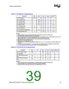
Table 26. Stop Grant/Sleep/Deep Sleep/Enhanced Intel SpeedStep Technology AC
Specifications
T# Parameter
Min
Max
Unit
Figure
Notes
T70: SLP# Signal Hold Time from Stop Grant
Cycle Completion
100
BCLKs
23
T71: Input Signals Stable to SLP# Assertion
T72: SLP# to DPSLP# Assertion
10
10
0
BCLKs
BCLKs
µs
23, 24
23
1
2
T73: Deep Sleep PLL Lock Latency
T74: SLP# Hold Time from PLL Lock
30
23
0
ns
23
T75: STPCLK# Hold Time from SLP#
Deassertion
10
10
0
BCLKs
BCLKs
µs
23
23, 24
24
T76: Input Signal Hold Time from SLP#
Deassertion
T77: VID[4:0] Output Valid Delay from DPSLP#
Assertion
10
NOTES:
1. Input signals other than RESET# must be held constant in the Sleep state.
2. The BCLK can be stopped after DPSLP# is asserted. The BCLK must be turned on and within specification
before DPSLP# is deasserted.
.
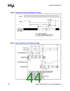
2.14
Processor AC Timing Waveforms
The following figures are used in conjunction with the AC timing tables, Table 19 through Table
26.
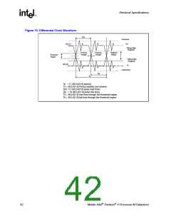
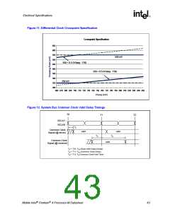
For Figure 9 through Figure 24, the following apply:
NOTES:
1. All common clock AC timings for AGTL+ signals are referenced to the Crossing Voltage (VCROSS) of the
BCLK[1:0] at rising edge of BCLK0. All common clock AGTL+ signal timings are referenced at GTLREF at the
processor core.
2. All source synchronous AC timings for AGTL+ signals are referenced to their associated strobe (address or
data) at GTLREF. Source synchronous data signals are referenced to the falling edge of their associated data
strobe. Source synchronous address signals are referenced to the rising and falling edge of their associated
address strobe. All source synchronous AGTL+ signal timings are referenced at GTLREF at the processor
core silicon.
3. All AC timings for AGTL+ strobe signals are referenced to BCLK[1:0] at VCROSS. All AGTL+ strobe signal
timings are referenced at GTLREF at the processor core silicon.
4. All AC timings for the TAP signals are referenced to the TCK signal at 0.5*VCC at the processor pins. All TAP
signal timings (TMS, TDI, etc.) are referenced at 0.5*VCC at the processor pins.
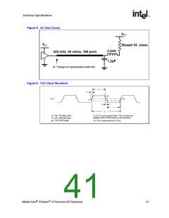
The circuit used to test the AC specifications is shown in Figure 8.
40
Mobile Intel Pentium 4 Processor-M Datasheet

 INTEL [ INTEL ]