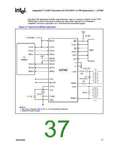
LXT362 — Integrated T1 LH/SH Transceiver for DS1/DSX-1 or PRI Applications
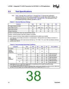
5.0
Test Specifications
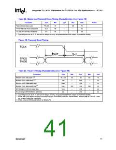
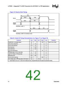
Note: Table 21 through Table 28 and Figure 14 through Figure 20 represent the performance
specifications of the LXT362 and are guaranteed by test except, where noted, by design. The
minimum and maximum values listed in Table 23 through Table 28 are guaranteed over the
recommended operating conditions specified in Table 22.
Table 21. Absolute Maximum Ratings
Parameter
Sym
Min
Max
Unit
DC supply (reference to GND)
Input voltage, any pin 1
Input current, any pin 2
Storage Temperature
VCC, TVCC
VIN
–
GND - 0.3 V
- 10
6.0
VCC + 0.3 V
10
V
V
IIN
mA
° C
TSTG
-65
150
Caution: Exceeding these values may cause permanent damage.
Caution: Functional operation under these conditions is not implied.
Caution: Exposure to maximum rating conditions for extended periods may affect device reliability.
1. TVCC and VCC must not differ by more than 0.3 V during operation. TGND and GND must not differ by more than 0.3 V
during operation.
2. Transient currents of up to 100 mA will not cause SCR latch-up. TTIP, TRING, TVCC, and TGND can withstand continuous
currents of up to 100 mA.
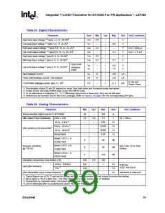
Table 22. Recommended Operating Conditions
Parameter
Sym
Min
Typ1
Max
Unit
Test Conditions
DC Supply 2
VCC, TVCC
4.75
5.0
5.25
V
Ambient
Operating
TA
-40
–
85
° C
Temperature
PD
PD
PD
PD
PD
PD
–
–
–
–
–
–
450
300
350
250
400
275
540
360
425
300
485
330
mW
mW
mW
mW
mW
mW
100% mark density
50% mark density
100% mark density
50% mark density
100% mark density
50% mark density
Short Haul
Long Haul
D4
Total
Power
Dissipation3
1. Typical figures are at 25 °C and are for design aid only; not guaranteed and not subject to production testing.
2. TVCC and VCC must not differ by more than 0.3 V.
3. Power dissipation while driving 100 Ω load over operating range. Includes power dissipation on device and load. Digital levels
are within 10% of the supply rails and digital outputs driving a 50 pF capacity load, R =9.1, T1=1:2.
L
38
Datasheet

 INTEL [ INTEL ]