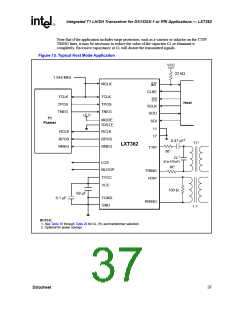
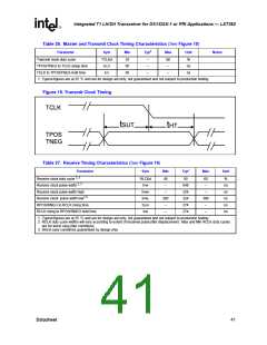
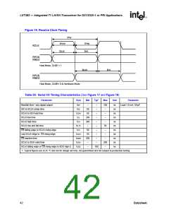
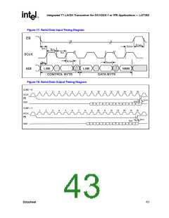
Integrated T1 LH/SH Transceiver for DS1/DSX-1 or PRI Applications — LXT362
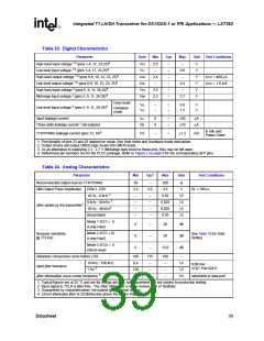
Table 23. Digital Characteristics
Parameter
Sym
Min
Typ
Max
Unit
Test Conditions
High level input voltage 1,2 (pins 1-4, 17, 23-25)4
Low level input voltage 1,2 (pins 1-4, 17, 23-25)4
High level output voltage 1,2 (pins 6-8, 10, 12, 23, 25)4
Low level output voltage 1,2 (pins 6-8, 10, 12, 23, 25)4
High level input voltage 3 (pins 5, 9, 11, 26-28)4
Midrange input voltage 3 (pins 5, 9, 11, 26-28)4
VIH
VIL
2.0
–
–
–
–
–
–
–
–
0.8
–
V
V
V
V
V
V
VOH
VOL
VIH
VIM
2.4
–
IOUT = 400 µA
0.4
–
IOUT = 1.6 mA
3.5
2.3
2.7
Host mode
VIL
VIL
–
–
–
–
0.8
1.5
V
V
Low level input voltage 3 (pins 5, 9, 11, 26-28)4
Hardware
mode
Input leakage current
ILL
0
0
–
–
±50
±10
µA
µA
Three-state leakage current 1 (all outputs)
I3L
in Idle and
Power Down
TTIP/TRING leakage current (pins 13, 16)4
ITR
–
–
±1.2
mA
1. Functionality of pins 23 and 25 depend on mode. See Host mode and Hardware mode description.
2. Output drivers will output CMOS logic levels into CMOS loads.
3. As an alternative to supplying 2.3 - 2.7 V (Midrange logic level) to these pins, they may be left open.
4. Referenced pin numbers are for the PLCC package. Refer to Figure 2 on page 8 for the corresponding QFP pins.
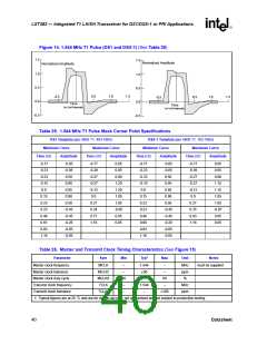
Table 24. Analog Characteristics
Parameter
Min
Typ1
Max
Unit
Test Conditions
Recommended output load on TTIP/TRING
50
2.4
–
–
3.0
–
200
3.6
Ω
V
AMI Output Pulse Amplitudes
Jitter added by the transmitter2
DSX-1, DS1
RL = 100 Ω
10 Hz - 8 kHz 3
8 kHz - 40 kHz 3
10 Hz - 40 kHz3
Broad Band
0.02
0.025
0.025
0.05
UI
UI
UI
UI
–
–
–
–
–
–
Mode 1 (EC1 = 1)
(Long-Haul)
0
0
0
–
–
–
26
36
dB
dB
dB
Mode 2 (EC1 = 0)
(Long-Haul)
Receiver sensitivity
@ 772 kHz
See Table 10 for Gain
Setting
Mode 3 (EC4 = 1)
(Short-Haul)
13.6
Allowable consecutive zeros before LOS
10 kHz - 100 kHz
1 Hz 3
Jitter attenuation curve corner frequency 4
160
0.4
138
–
175
–
190
–
–
UI
UI
Hz
0 dB line
AT&T Pub 62411
Input jitter tolerance
–
–
3
–
selectable in data port
1. Typical figures are at 25 °C and are for design aid only; not guaranteed and not subject to production testing.
2. Input signal to TCLK is jitter-free. The Jitter Attenuator is in the receive path or disabled.
3. Guaranteed by characterization; not subject to production testing.
4. Circuit attenuates jitter at 20 dB/decade above the corner frequency.
Datasheet
39

 INTEL [ INTEL ]