Integrated T1 LH/SH Transceiver for DS1/DSX-1 or PRI Applications — LXT362
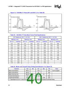
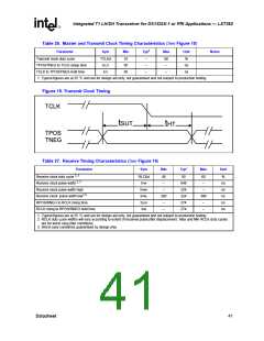
Table 26. Master and Transmit Clock Timing Characteristics (See Figure 15)
Parameter
Sym
Min
Typ1
Max
Unit
Notes
Transmit clock duty cycle
TCLKd
tSUT
10
50
50
–
–
–
90
–
%
ns
ns
TPOS/TNEG to TCLK setup time
TCLK to TPOS/TNEG hold time
tHT
–
1. Typical figures are at 25 °C and are for design aid only; not guaranteed and not subject to production testing.
Figure 15. Transmit Clock Timing
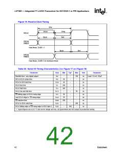
Table 27. Receive Timing Characteristics (See Figure 16)
Parameter
Receive clock duty cycle 2, 3
Sym
Min
Typ1
Max
Unit
RLCKd
tPW
40
–
50
60
–
%
ns
ns
ns
ns
ns
Receive clock pulse width 2, 3
648
324
324
274
274
Receive clock pulse width high
Receive clock pulse width low1,3
RPOS/RNEG to RCLK rising time
RCLK rising to RPOS/RNEG hold time
tPWH
tPWL
tSUR
tHR
–
–
260
–
388
–
–
–
1. Typical figures are at 25 °C and are for design aid only; not guaranteed and not subject to production testing.
2. RCLK duty cycle widths will vary according to extent of received pulse jitter displacement. Max and Min RCLK duty cycles
are for worst case jitter conditions.
3. Worst case conditions guaranteed by design only.
Datasheet
41

 INTEL [ INTEL ]