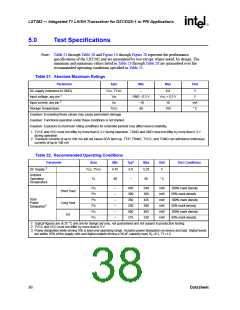
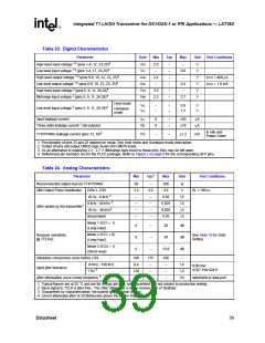
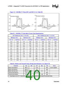
LXT362 — Integrated T1 LH/SH Transceiver for DS1/DSX-1 or PRI Applications
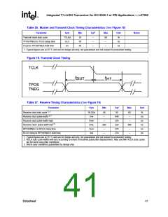
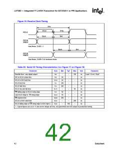
Figure 16. Receive Clock Timing
,
,
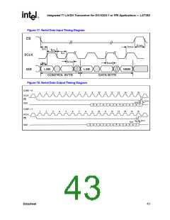
Table 28. Serial I/O Timing Characteristics (See Figure 17 and Figure 18)
Parameter
Sym
Min
Typ1
Max
Unit
Parameter
Rise/fall time—any digital output
SDI to SCLK setup time
tRF
tDC
–
50
50
240
240
–
–
–
100
–
ns
ns
ns
ns
ns
ns
ns
ns
ns
ns
ns
Load 1.6 mA, 50 pF
SCLK to SDI hold time
tCDH
tCL
–
–
SCLK low time
–
–
SCLK high time
tCH
–
–
SCLK rise and fall time
tR, tF
tCC
–
50
–
CS falling edge to SCLK rising edge
Last SCLK edge to CS rising edge
CS inactive time
50
50
250
–
–
tCCH
tCWH
tCDV
tCDZ
–
–
–
–
SCLK to SDO valid time
–
200
–
SCLK falling edge or CS rising edge to SDO high-Z
–
100
1. Typical figures are at 25 °C and are for design aid only; not guaranteed and not subject to production testing.
42
Datasheet

 INTEL [ INTEL ]