Integrated T1 LH/SH Transceiver for DS1/DSX-1 or PRI Applications — LXT362
In Hardware mode, the ES is a 32 x 2-bit register. Setting the JASEL pin High places the JA
circuitry in the receive data path; setting JASEL Low places the JA in the transmit data path;
setting it to Midrange disables the JA.
In Host mode, bit CR1.JASEL0 enables or disables the JA circuit while bit CR1.JASEL1 controls
the JA circuit placement as specified in Table 9 on page 30. The ES can be either a 32 x 2-bit or 64
x 2-bit register depending on the value of bit CR3.ES64 (see Table 12).
The device clocks data into the ES using either TCLK or RCLK depending on whether the JA
circuitry is in the transmit or receive data path, respectively. Data is shifted out of the elastic store
using the dejittered clock from the JAL. When the FIFO is within two bits of overflowing or
underflowing, the ES adjusts the output clock by 1/ of a bit period. The ES produces an average
8
delay of 16 bits in the data path. An average delay of 32 bits occurs when the 64-bit ES option
selected (Host mode only). In the event of a LOS condition, with the Jitter Attenuator in the receive
path, RCLK will be derived from MCLK.
Transition Status Register bits TSR.ESOVR and TSR.ESUNF indicate an elastic store overflow or
underflow, respectively. Note that these are “sticky bits”, that is, once set to 1, they remain set until
the host reads the register. An ES overflow or underflow condition will generate a maskable
interrupt.
2.5
2.6
Hardware Mode
The LXT362 operates in Hardware mode when the MODE pin is set to Low or Midrange. In
Hardware mode individual pins are used to access and control the transceiver. In Hardware mode,
RPOS/RNEG or RDATA are valid on the rising edge of RCLK.
Note that some functions, such as interrupt (INT), clock edge selection (CLKE), and various
diagnostic modes, are provided only in Host mode.
Host Mode
The LXT362 operates in Host mode when the MODE pin is set High. In Host mode a
microprocessor controls the LXT362 and reads its status via the serial port which provides access
to the LXT362’s internal registers.
The host microprocessor can completely configure the device, as well as get a full diagnostic/status
report, via the serial port. However, in Unipolar mode, bipolar violation (BPV) insertions and logic
error insertions are controlled by the BPV and INSLER pins, respectively. Similarly, the recovered
clock, data, and BPV detection are available only at output pins. All other mode settings and
diagnostic information are available via the serial port. See “Register Definitions” on page 29 for
details.
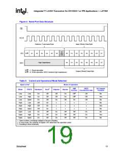
Figure 4 shows the serial port data structure. The registers are accessible through a 16-bit word
composed of an 8-bit Command/Address byte (bits R/W and A1-A7) and a subsequent 8-bit data
byte (bits D0-7). The R/W bit commands a read or a write operation, i.e., the direction of the
following byte. Bits A1 through A6, of the command/address byte, point to a specific register. Note
that the LXT362 address decoder ignores bits A0 and A7. Refer to Table 28 on page 42 for timing
specifications.
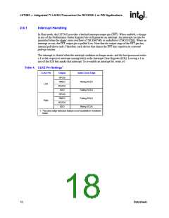
Host mode also allows control of data output timing. The CLKE pin determines when SDO is
valid, relative to the Serial Clock (SCLK) as shown in Table 4.
Datasheet
17

 INTEL [ INTEL ]