LXT362 — Integrated T1 LH/SH Transceiver for DS1/DSX-1 or PRI Applications
2.6.1
Interrupt Handling
In Host mode, the LXT362 provides a latched interrupt output pin (INT). When enabled, a change
in any of the Performance Status Register bits will generate an interrupt. An interrupt can also be
generated when the elastic store overflows (TSR.ESOVR) or underflows (TSR.ESUNF). When an
interrupt occurs, the INT output pin is pulled Low. Note that the output stage of the INT pin has
internal pull-down only. Therefore, each device that shares the INT line requires an external
pull-up resistor.
The interrupt is cleared when the interrupt condition no longer exists, and the host processor writes
a 1 to the respective interrupt causing bit(s) in the Interrupt Clear Register (ICR). Leaving a 1 in
any of the ICR bits masks that interrupt. To re-enable an interrupt bit, write a 0.
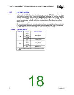
Table 4. CLKE Pin Settings1
CLKE Pin
Output
Valid Clock Edge
RPOS
RNEG
RDATA
SDO
Rising RCLK
Falling SCLK
Falling RCLK
Rising SCLK
Low
RPOS
RNEG
RDATA
SDO
High
1. The clock edge selection feature is not available in Hardware
mode.
18
Datasheet

 INTEL [ INTEL ]