Integrated T1 LH/SH Transceiver for DS1/DSX-1 or PRI Applications — LXT362
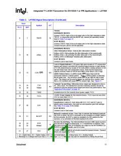
Table 3. LXT362 Signal Descriptions (Continued)
Pin #
PLCC
Symbol
I/O1
Description
QFP
HARDWARE MODES:
Local Loopback. When held High, the data on TPOS and TNEG loops
back digitally to the RPOS and RNEG outputs (through the JA if enabled).
Connecting this pin to Midrange2 enables Analog loopback (TTIP and
TRING are looped back to RTIP and RRING).
27
37
LLOOP / SCLK
DI
HOST MODES:
Serial Clock. SCLK synchronizes serial port read/write operations. The
clock frequency can be any rate up to 2.048 MHz.
HARDWARE MODES:
Transmit All Ones. When held High, the transmit data inputs are ignored
and the LXT362 transmits a stream of 1’s at the TCLK frequency. If TCLK
is not supplied, MCLK becomes the transmit clock reference. Note that
TAOS is inhibited during Remote loopback.
QRSS. In QRSS mode, setting this pin to Midrange2, enables QRSS
pattern generation and detection. The transceiver transmits the QRSS
pattern at the TCLK rate (or MCLK, if TCLK is not present).
TAOS / QRSS /
CLKE
28
38
DI
HOST MODES:
Clock Edge Select. When CLKE is High, RPOS/RNEG or RDATA are
valid on the falling edge of RCLK, and SDO is valid on the rising edge of
SCLK.
When CLKE is Low, RPOS/RNEG or RDATA are valid on the rising edge of
RCLK, and SDO is valid on the falling edge of SCLK. The operation of
CLKE is summarized in Table 4 on page 18.
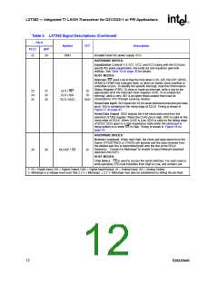
1, 6, 8,
9, 11,
12, 14,
17, 22,
23, 26,
28, 30,
33, 34,
40, 44
10
n/c
-
Not Connected
1. DI = Digital Input; DO = Digital Output; DI/O = Digital Input/Output; AI = Analog Input; AO = Analog Output.
2. Midrange is a voltage level such that 2.3 V ≤ Midrange ≤ 2.7 V. Midrange may also be established by letting the pin float.
Datasheet
13

 INTEL [ INTEL ]