Integrated T1 LH/SH Transceiver for DS1/DSX-1 or PRI Applications — LXT362
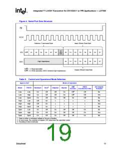
Figure 4. Serial Port Data Structure
CS
SCLK
Address / Command Byte
Input (Write) Data Byte
A7
(don’t
care)
R/W
A1
A2
A3
A4
A5
A6
D0
D0
D1
D1
D2
D2
D3
D3
D4
D4
D5
D5
D6
D6
D7
D7
SDI
High Impedance
SDO
R/W = 1: Read operation
R/W = 0: Write operation (SDO remains high impedance)
Output (Read) Data Byte
.
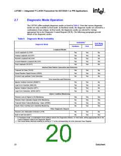
Table 5. Control and Operational Mode Selection
Input to Pin1
Mode of Operation
AMI
B8ZS
All Outputs
Tristated
Mode
TRSTE
Hardware
Host2
Unipolar
Bipolar
Enc/Dec Encoder/Decoder
Low
Low
Low
High
Open
Low
On
On
On
Off
Off
Off
On
On
On
Off
Off
Off
On
On
On
Off
Off
Off
Off
Off
On
x
On
On
Off
x
Off3
Off3
On
x
Off
Off
Off
x
No
Yes
No
Low
High
High
High
Open
Open
Open
No
High
Open
Low
x
x
x
x
Yes
No
x
x
x
x
On
On
On
Off
Off
Off
Off
Off
Off
On
On
On
No
High
Open
Yes
No
1. Open is either a midrange voltage or the pin is floating.
2. In Host mode, the contents of register CR1 determine the operation mode.
3. Encoding is done externally.
Datasheet
19

 INTEL [ INTEL ]