XMC4500
XMC4000 Family
Electrical Parameters
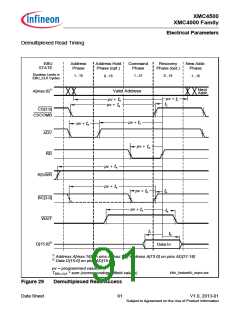
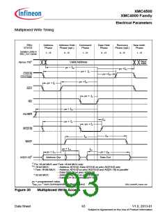
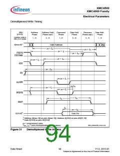
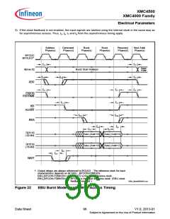
3.3.10.2 EBU Burst Mode Access Timing
Note: These parameters are not subject to production test, but verified by design and/or
characterization.
Note: Operating Conditions apply, with Class A2 pins and CL = 16 pF.
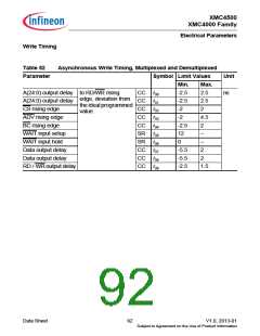
Table 53
EBU Burst Mode Read / Write Access Timing Parameters
Parameter
Symbol
Values
Unit Note /
Test Condition
Min. Typ. Max.
Output delay from BFCLKO t10 CC -2
rising edge
–
2
ns
ns
–
RD and RD/WR
t12 CC -2
–
2
–
active/inactive after
BFCLKO active edge1)
CSx output delay from
BFCLKO active edge1)
t21
t22
CC -2.5
CC -2
–
–
–
–
–
–
–
1.5
2
ns
ns
ns
ns
ns
ns
ns
–
–
–
–
–
–
–
ADV active/inactive after
BFCLKO active edge2)
BAA active/inactive after
BFCLKO active edge2)
t22a CC -2.5
1.5
–
Data setup to BFCLKI rising t23
SR
SR
SR
SR
3
0
3
0
edge3)
Data hold from BFCLKI
rising edge3)
t24
–
WAIT setup (low or high) to t25
–
BFCLKI rising edge3)
WAIT hold (low or high) from t26
–
BFCLKI rising edge3)
1) An active edge can be a rising or falling edge, depending on the settings of bits BFCON.EBSE / ECSE and
the clock divider ratio.
Negative minimum values for these parameters mean that the last data read during a burst may be corrupted.
However, with clock feedback enabled, this value is an oversampling not required for the internal bus
transaction, and will be discarded.
2) This parameter is valid for BUSCONx.EBSE = 1 and BUSAPx.EXTCLK = 00B.
For BUSCONx.EBSE = 1 and other values of BUSAPx.EXTCLK, ADV and BAA will be delayed by 1/2 of the
internal bus clock period TCPU = 1 / fCPU
.
For BUSCONx. EBSE = 0 and BUSAPx.EXTCLK = 11B, add 2 internal bus clock periods.
For BUSCONx. EBSE = 0 and other values of BUSAPx.EXTCLK, add 1 internal bus clock period.
Data Sheet
95
V1.0, 2013-01
Subject to Agreement on the Use of Product Information

 INFINEON [ Infineon ]