XMC4500
XMC4000 Family
Electrical Parameters
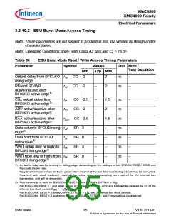
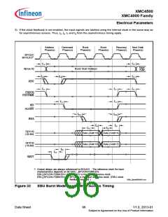
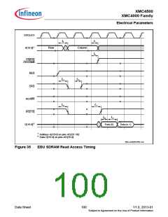
3) If the clock feedback is not enabled, the input signals are latched using the internal clock in the same way as
for asynchronous access. Thus, t5, t6, t7 and t8 from the asynchronous timing apply.
Address
Phase(s)
Command
Phase(s)
Burst
Phase(s)
Burst
Phase(s)
Recovery
Phase(s)
Next Addr.
Phase(s)
BFCLKI
BFCLKO1)
t10
t10
Next
A[max :0]
ADV
Burst Start Address
Addr.
t22
t22
t22
t21
t21
t21
CS[3:0]
CSCOMB
t12
t12
RD
RD/WR
t22a
t22a
BAA
t24
t24
t23
t23
D[31:0]
(32-Bit)
Data (Addr+0)
Data (Addr+4)
D[15:0]
(16-Bit)
Data (Addr+0)
Data (Addr+2)
t26
t25
WAIT
1)
Output delays are always referenced to BCLKO . The reference clock for input
characteristics depends on bit EBU _BFCON.FDBKEN.
EBU_BFCON.FDBKEN= 0: BFCLKO is the input reference clock .
EBU_BFCON.FDBKEN= 1: BFCLKI is the input reference clock (EBU clock
feedback enabled ).
EBU_BurstRDWR.vsd
Figure 32
EBU Burst Mode Read / Write Access Timing
Data Sheet
96
V1.0, 2013-01
Subject to Agreement on the Use of Product Information

 INFINEON [ Infineon ]