XMC4500
XMC4000 Family
Electrical Parameters
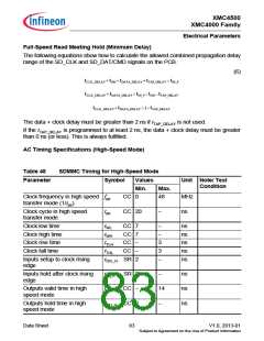
Table 49
SD Card Bus Timing for High-Speed Mode1)
Parameter
Symbol
Values
Unit Note/ Test
Condition
Min.
6
Max.
SD card input setup time
SD card input hold time
SD card output valid time
SD card output hold time
tISU
tIH
tODLY
tOH
−
ns
ns
ns
ns
2
−
−
14
2.5
−
1) Reference card timing values for calculation examples. Not subject to production test and not characterized.
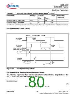
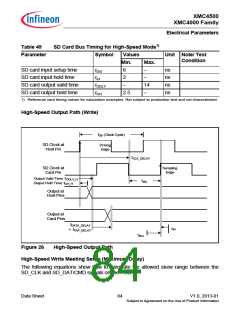
High-Speed Output Path (Write)
tpp (Clock Cycle)
SD Clock at
Host Pin
Driving
Edge
tCLK_DELAY
SD Clock at
Card Pin
Sampling
Edge
Output Valid Time: tODLY_H
Output Hold Time: tOH_H
tWL
Output at
Host Pins
Output at
Card Pins
tDATA_DELAY
+ tTAP_DELAY
tIH
tISU
Figure 26
High-Speed Output Path
High-Speed Write Meeting Setup (Maximum Delay)
The following equations show how to calculate the allowed skew range between the
SD_CLK and SD_DAT/CMD signals on the PCB.
Data Sheet
84
V1.0, 2013-01
Subject to Agreement on the Use of Product Information

 INFINEON [ Infineon ]