XMC4500
XMC4000 Family
Electrical Parameters
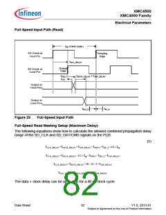
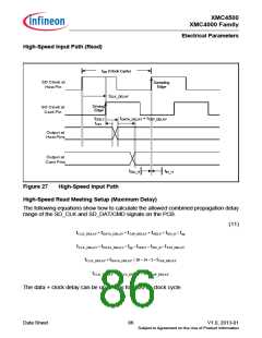
High-Speed Input Path (Read)
tpp (Clock Cycle)
SD Clock at
Host Pin
Sampling
Edge
tCLK_DELAY
Driving
Edge
SD Clock at
Card Pin
tODLY
tOH
tDATA_DELAY + tTAP_DELAY
Output at
Host Pins
Output at
Card Pins
tISU_H
tIH_H
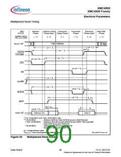
Figure 27
High-Speed Input Path
High-Speed Read Meeting Setup (Maximum Delay)
The following equations show how to calculate the allowed combined propagation delay
range of the SD_CLK and SD_DAT/CMD signals on the PCB.
(11)
tCLK_DELAY + tDATA_DELAY + tTAP_DELAY + tODLY + tISU_H < tpp
tCLK_DELAY + tDATA_DELAY < tpp – tODLY – tISU_H – tTAP_DELAY
tCLK_DELAY + tDATA_DELAY < 20 – 14 – 2 – tTAP_DELAY
tCLK_DELAY + tDATA_DELAY < 4 – tTAP_DELAY
The data + clock delay can be up to 4 ns for a 20 ns clock cycle.
Data Sheet
86
V1.0, 2013-01
Subject to Agreement on the Use of Product Information

 INFINEON [ Infineon ]