XMC4500
XMC4000 Family
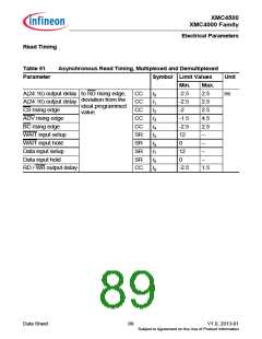
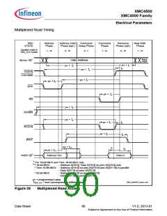
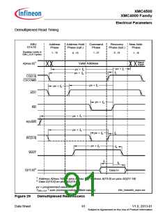
Electrical Parameters
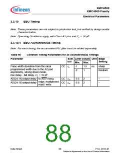
3.3.10
EBU Timing
Note: These parameters are not subject to production test, but verified by design and/or
characterization.
Note: Operating Conditions apply, with Class A2 pins and CL = 16 pF.
3.3.10.1 EBU Asynchronous Timing
Note: For each timing, the accumulated PLL jitter must be added separately.
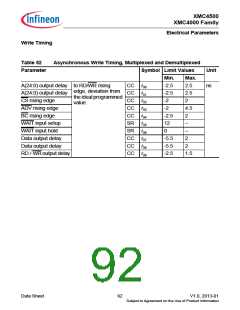
Table 50
Common Timing Parameters for all Asynchronous Timings
Sym Limit Values Unit Edge
Parameter
bol
Setting
Min. Max.
Pulse width deviation from the ideal
programmed width due to the A2 pad
asymmetry, strong driver mode,
rise delay - fall delay. CL = 16 pF.
CC ta
-1
-2
1.5
1
ns
sharp
medium
AD(24:16) output delay to ADV rising
CC t13
CC t14
-5.5
-5.5
2
2
–
–
edge, multiplexed
AD(24:16) output delay
read / write
Data Sheet
88
V1.0, 2013-01
Subject to Agreement on the Use of Product Information

 INFINEON [ Infineon ]