XMC4500
XMC4000 Family
Electrical Parameters
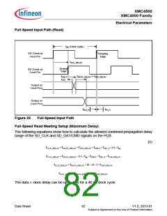
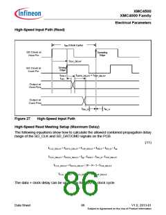
Full-Speed Read Meeting Hold (Minimum Delay)
The following equations show how to calculate the allowed combined propagation delay
range of the SD_CLK and SD_DAT/CMD signals on the PCB.
(6)
tCLK_DELAY + tOH + tDATA_DELAY + tTAP_DELAY > tIH_F
tCLK_DELAY + tDATA_DELAY > tIH_F – tOH – tTAP_DELAY
tCLK_DELAY + tDATA_DELAY > 2 – tTAP_DELAY
The data + clock delay must be greater than 2 ns if tTAP_DELAY is not used.
If the tTAP_DELAY is programmed to at least 2 ns, the data + clock delay must be greater
than 0 ns (or less). This is always fulfilled.
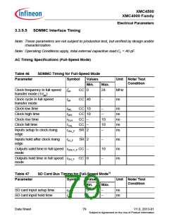
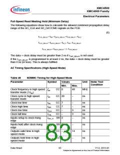
AC Timing Specifications (High-Speed Mode)
Table 48
SDMMC Timing for High-Speed Mode
Parameter
Symbol
Values
Min.
Unit Note/ Test
Condition
Max.
Clock frequency in high speed fpp
transfer mode (1/tpp)
CC 0
48
MHz
ns
Clock cycle in high speed
transfer mode
tpp
CC 20
−
Clock low time
Clock high time
Clock rise time
Clock fall time
tWL
CC 7
CC 7
CC −
CC −
−
−
3
3
−
ns
ns
ns
ns
ns
tWH
tTLH
tTHL
Inputs setup to clock rising
edge
tISU_H SR 2
Inputs hold after clock rising
edge
tIH_H SR 2
−
ns
ns
ns
Outputs valid time in high
speed mode
tODLY_H CC −
14
−
Outputs hold time in high
speed mode
tOH_H CC 2
Data Sheet
83
V1.0, 2013-01
Subject to Agreement on the Use of Product Information

 INFINEON [ Infineon ]