Forced Quasi Resonant ZVS flyback controller
Functional Description
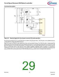
vDrain(t)
NPri / NSec × vSec
VBulk
t
Forced frequency
resonant mode
vZVS(t)
NZVS / NSec × vSec
0
t
NZVS / NPri × VBulk
iMag(t)
tf
tZVSdelay
0
t
t
vGD0(t)
tSWperiod
tGD0On
tGD0Off
vGD1(t)
tZVSdead
tGD1on
tGD1Off
t
t1 t2 t3
t4
t5
t1 t2 t3
t4
FFR_MODE_SIGNALS
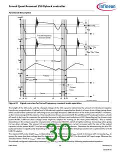
Figure 29 Signal overview for forced frequency resonant mode operation
The length of the ZVS pulse and the charged voltage of the ZVS capacitor determine the amount of introduced negative
transformer magnetization. A higher level of introduced negative magnetization leads to a lower drain voltage swing down,
which could further optimize the switching losses and high frequency EMI behavior of the main power MOSFET. However,
as this comes along with the expense of increased power losses associated with the additional ZVS pulse generation, a trade
off needs to be found to maximize the potential increase in efficiency and reduction in EMI. Depending on the chosen main
power MOSFET different drain voltage levels might be adapted for turning on the main power MOSFET. This is mainly
depending on the output capacitor characteristic of the power MOSFET, which is highly nonlinear increasing, when going
for low drain voltages. The amount of necessary negative magnetization current increases with the size of the output
capacitor of the power MOSFET and parasitic coupling capacitor of transformer. Therefore the dimensioning for the ZVS
pulse generation is significantly depending on the system dimensioning. The default parameter set is optimized for a 65 W
USB PD adapter.
The required ZVS pulse length tGD1on is depending on VBulk. The GD1 on-time tGD1on needs to increase with increasing VBulk to
ensure the same low drain voltage level for turning on the main power MOSFET for the whole VAC input range. Whereas the
ZVS dead-time is fixed at tZVSdead = 236ns (see Chapter 5.2 ).
The default configured relationship between tGD1on and VBulk and determined by following implemented equation:
Data Sheet
30
Revision 2.0
2020-08-20

 INFINEON [ Infineon ]