Forced Quasi Resonant ZVS flyback controller
Functional Description
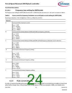
160
140
120
100
80
min Fsw
max Fsw
CRCM
QR-1
QR-2
QR-3
60
QR-4
QR-5
40
QR-6
20
0
0
100
200
300
400
VCSpk [mV]
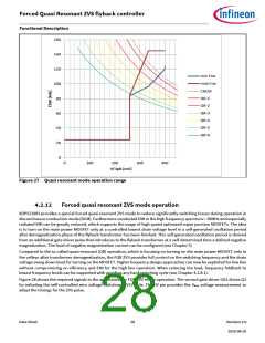
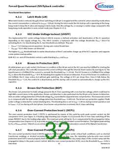
Figure 27 Quasi resonant mode operation range
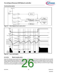
4.2.12
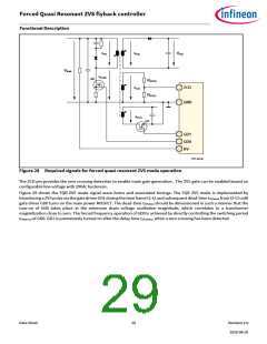
Forced quasi resonant ZVS mode operation
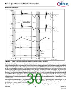
XDPS21081 provides a special forced quasi resonant ZVS mode to reduce significantly switching losses during operation in
discontinuous conduction mode (DCM). Furthermore conducted EMI in the high frequency spectrum > 10MHz and especially
radiated EMI can be greatly reduced, which supports the usage of high speed optimized super junction MOSFETs. The idea
is to turn on the main power MOSFET only at a controlled lowest drain voltage level in a self-generated oscillation period
after demagnetization phase of the flyback transformer has been finished. This self-generated oscillation period is derived
from an additional gate driver pulse that introduces to the flyback transformer at a self-determined time a defined negative
magnetization. The level of negative magnetization current can be configured (see Chapter 5)
Compared to the so called quasi-resonant (QR) operation, which is focusing on turning on the main power MOSFET only in
the valleys after transformer demagnetization, the FQR ZVS provides full control on the switching frequency and the drain
voltage swing down level for turning on the MOSFET. Higher frequency design approaches can now be exploited for low line
without compromising on efficiency and EMI for the high line operation. When reducing the load, frequency foldback to
lowest frequency levels can be supported with avoiding any hard switching cycle (see Chapter 4.2.8.1).
Figure 28 shows the required signals in the application for FQR ZVS mode operation. The second gate driver GD1 drives Q1
for initiating the self-controlled zero voltage switching (ZVS) cycle. The HV pin provides the VBulk voltage measurement to
adapt the timings for the ZVS pulse.
Data Sheet
28
Revision 2.0
2020-08-20

 INFINEON [ Infineon ]