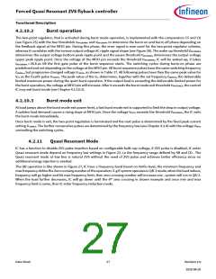
Forced Quasi Resonant ZVS flyback controller
Functional Description
vPri
vSec
VOut
VBulk
vDrain
Q0
RZCDH
vAux
ZCD
GND
RZCDL
vZVS
Q1
GD1
GD0
HV
FFR MODE
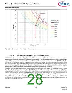
Figure 28 Required signals for forced quasi resonant ZVS mode operation
The ZCD pin provides the zero crossing detection to enable main gate generation. The ZVS gate can be enabled based on
configurable line voltage with 20Vdc hysteresis.
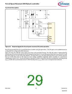
Figure 29 shows the FQR ZVS mode signal wave forms and associated timings. The FQR ZVS mode is implemented by
introducing a ZVS pulse via the gate driver GD1 during the time frame t1-t2 and subsequent dead-time tZVSdead from t2-t3 until
gate driver GD0 turns on the main power MOSFET. The dead-time tZVSdead should be dimensioned in such a manner that the
turn-on of GD0 takes place at the minimum drain voltage oscillation magnitude, which correlates to a transformer
magnetization close to zero. The forced frequency operation of GD0 is achieved by directly controlling the switching period
tSWperiod of GD0. GD1 is prematurely turned on after the delay time tZVSdelay, when a zero crossing has been detected.
Data Sheet
29
Revision 2.0
2020-08-20

 INFINEON [ Infineon ]