Forced Quasi Resonant ZVS flyback controller
Functional Description
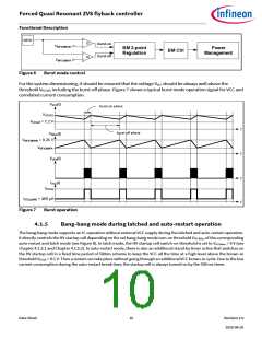
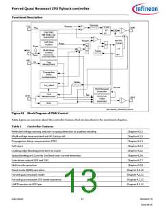
4.2.1
Reflected voltage sensing and VCS offset calculation based on
output voltage
The IC provides output voltage detection by means of measuring the reflected voltage at the auxiliary winding VAux at the
primary side of the transformer via ZCD pin and an external resistive voltage divider. The voltage signal VAux contains the
information of the flyback output voltage, VOut, at the secondary side.
The ZCD pin related circuit is shown in Figure 12. Figure 13 shows a typical voltage waveform of the drain voltage VDrain and
the related auxiliary winding voltage VAux. The sensed output voltage is used for over-voltage protection (see Chapter 4.3.11).
Following topics are described in the sequel:
•
•
Output voltage sensing via ZCD pin (Chapter 4.2.1.1)
Vcs offset with sensed Vo at ZCD pin (Chapter 4.2.1.3)
vPri
vSec
VOut
VBulk
vDrain
RZCDH
iZCD
vZCD
vAux
ZCD
GND
RZCDL
vZVS
VOLTAGE_SENSING_OVERVIEW
Figure 12 Functionality at ZCD pin
Data Sheet
14
Revision 2.0
2020-08-20

 INFINEON [ Infineon ]