Forced Quasi Resonant ZVS flyback controller
Functional Description
tCSOCP2BL
CS
VCSOCP2
CLEAR
VCS
GD0
+
&
FF
Cold Start,
BM Wake-Up,
Autorestart
SET
&
+
stop GD0
VCSOCP1
Soft-Start
Control
CLEAR
VCSSS
&
M
I
N
VVDDP
FF
Multi-Mode
Control
frequency law,
burst mode control
MFIO
HV
tCSLEB
SET
VMFIO
IHV
VBulk
Measurment
Propagation
Delay
Compensation
tZCDRS
Vcs_offset
start GD0
Start Request
Generator
Vout
Measurement
fSW
ZCD
FFR ZVS
PWM
GD1
Generator
ZCD
MULTIMODE_OVERVIEW_DIGITAL
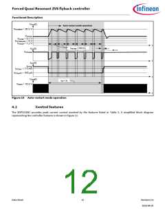
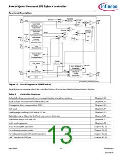
Figure 11 Block Diagram of PWM Control
Table 2 gives an overview about the controller features that are described in the mentioned chapters.
Table 2
Controller Features
Reflected voltage sensing and zero crossing detection at auxiliary winding
Vbulk voltage measurement via HV startup cell
Propagation delay compensation (PDC)
Soft-start
Chapter 4.2.1
Chapter 4.2.2
Chapter 4.2.3
Chapter 4.2.4
Chapter 4.2.5
Chapter 4.2.6
Chapter 4.2.7
Chapter 4.2.8
Chapter 4.2.10
Chapter 4.2.11
Chapter 4.2.12
Chapter 4.2.13
Leading edge blanking (LEB) time at CS pin
Spike blanking at CS pin for 2nd level over-current detection
Gate driver output GD0 and GD1
Multi-mode operation
Burst mode (QBM) operation
Forced quasi resonant mode
Forced quasi resonant ZVS mode operation
UART function at GPIO pin
Data Sheet
13
Revision 2.0
2020-08-20

 INFINEON [ Infineon ]