TLD7002-16ES
Datasheet
6 Power Stage
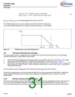
IOUT − 5 . 625mA
kDER
=
(2)
TJDER
TJstart = TJstop - TJDER, where TJDER is configured globally and is stored in the OTP.
TJDER is programmable by a 3-bit register with 5 options as shown below with an accuracy of aTJDER for each step:
Table 14
Thermal derating configuration
TJDER step
TJDER temperature
0
1
2
3
4
20°C
30°C
40°C
50°C
60°C
The thermal derating function can be enabled or disabled via the OTP configuration.
In case the thermal derating feature is enable, the power shif feature is not available.
IOUT
TJstop-TJDER(4)
TJstop-TJDER(0)
TJDER
TJ
TJ
TJstart
stop TJ(ABS)
Figure 10
Thermal derating
Thermal derating it is an integrated protection feature intended to avoid a light off condition at high junction
temperature.
The output current is reduced applying discrete current steps, with magnitude depending on the thermal derating
configuration.
Optical performance and perceived light variation during derating has to be tested in the final application.
The device provide the value of the internal temperature sensor in the DTS status register.
The sensor is not reading the peak junction temperature but an average die temperature.
6.8.2
Thermal derating with GPIN0
The output stage provides a configurable derating of the output current based on the voltage on GPIN0. Each output
stage starts to decrease the current linearly when VGPIN0 ≥ VDER_start until VDER_stop is reached, where
Datasheet
30
Rev.1.00
2022-05-03

 INFINEON [ Infineon ]