TC39x BC/BD-Step
Electrical SpecificationEBU Timings
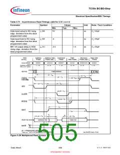
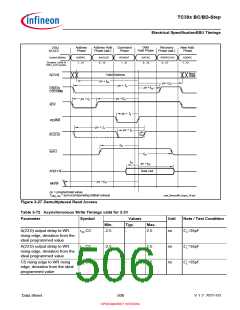
Table 3-72 Asynchnronous Write Timings valid for 3.3V (cont’d)
Parameter
Symbol
Values
Typ.
Unit
Note / Test Condition
Min.
Max.
ADV rising edge to WR rising
edge, deviation from the ideal
programmed value
t
t
t
t
t
t
t
33 CC
34 CC
35 SR
36 SR
37 CC
38 CC
39 CC
-2.5
-
-
-
-
-
-
-
2
ns
CL=35pF
BC rising edge to WR rising
edge, deviation from the ideal
programmed value
-2.5
19
2
ns
ns
ns
ns
ns
ns
CL=35pF
CL=35pF
CL=35pF
CL=35pF
CL=35pF
CL=35pF
WAIT input setup to WR rising
edge, deviation from the ideal
programmed value
-
WAIT input hold to WR rising
edge, deviation from the ideal
programmed value
0
-
Data output delay to WR rising
edge, deviation from the ideal
programmed value
-5.5
-5.5
-2.5
2.5
2.5
1.5
Data output delay to WR rising
edge, deviation from the ideal
programmed value
MR / W output delay to WR
rising edge, deviation from the
ideal programmed value
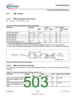
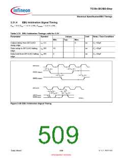
3.31.3
EBU Burst Mode Access Timing
VSS = 0 V;VDD = 1.3 V ± 5%; VDDEBU = 3.3 V ± 5%;
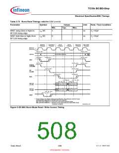
Table 3-73 Burst Read Timings valid for 3.3V
Parameter
Symbol
Values
Unit
Note / Test Condition
Min.
Typ.
Max.
Output delay from BFCLKO
rising edge
t
t
10 CC
12 CC
-2
-
2.5
ns
ns
ns
ns
ns
ns
ns
CL=35pF
CL=35pF
CL=35pF
CL=35pF
CL=35pF
CL=35pF
CL=35pF
RD and RD/WR active/inactive
after BFCLKO active edge
-2
-
-
-
-
-
-
2
CSx output delay from BFCLKO t21 CC
active edge
-2.5
-2
2.0
2
ADV active/inactive after
BFCLKO active edge
t
t
t
t
22 CC
22a CC
23 SR
24 SR
BAA active/inactive after
BFCLKO active edge
-2.5
5
2.0
-
Data setup to BFCLKI rising
edge
Data hold from BFCLKI rising
edge
0
-
Data Sheet
507
V 1.2, 2021-03
OPEN MARKET VERSION

 INFINEON [ Infineon ]