TC39x BC/BD-Step
Electrical SpecificationEBU Timings
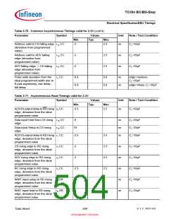
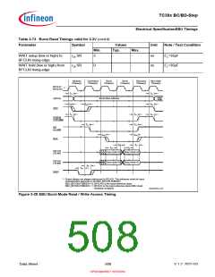
Table 3-70 Common Asynchronous Timings valid for 3.3V (cont’d)
Parameter Symbol Values
Typ.
Unit
Note / Test Condition
Min.
Max.
Address valid to CS falling edge t15 CC
(deviation from programmed
value)
-2
-
-
-
2.5
ns
CL=35pF
Address valid to ADV falling
edge (deviation from
t
16 CC
-2
-2
2.5
2.5
ns
ns
CL=35pF
CL=35pF
programmed value)
ADV falling edge -> CS falling
edge (deviation from
t
17 CC
programmed value)
Pulse wdih deviation from the
ideal programmed width due to
B pad asymmetry, rise delay -
fall delay
ta CC
-0.8
-0.8
-
-
0.8
0.8
ns
ns
edge=medium;
CL=35pF
edge=sharp; CL=35pF
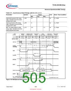
Table 3-71 Asynchronous Read Timings valid for 3.3V
Parameter Symbol
Values
Unit
Note / Test Condition
Min.
Typ.
Max.
A(23:0) output delay to RD rising t0 CC
edge, deviation from the ideal
programmed value
-2.5
-
2.5
ns
CL=35pF
Data input Hold from CS rising
edge
t
18 CC
-6
-
-
-
-
ns
ns
ns
CL=35pF
CL=35pF
CL=35pF
Data input Setup to CS rising
edge
t
19 CC
19
-
A(23:0) output delay to RD rising t1 CC
edge, deviation from the ideal
programmed value
-2.5
2.5
CS rising edge to RD rising
edge, deviation from the ideal
programmed value
t2 CC
t3 CC
t4 CC
t5 SR
t6 SR
-2
-
-
-
-
-
2.5
4.5
2.5
-
ns
ns
ns
ns
ns
CL=35pF
CL=35pF
CL=35pF
CL=35pF
CL=35pF
ADV rising edge to RD rising
edge, deviation from the ideal
programmed value
-2
BC rising edge to RD rising
edge, deviation from the ideal
programmed value
-2.5
19
-4
WAIT input setup to RD rising
edge, deviation from the ideal
programmed value
WAIT input hold to RD rising
edge, deviation from the ideal
programmed value
-
Data Sheet
504
V 1.2, 2021-03
OPEN MARKET VERSION

 INFINEON [ Infineon ]