S29GL01GP
S29GL512P
S29GL256P
S29GL128P
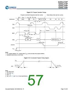
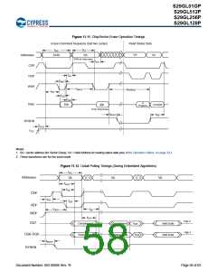
Figure 11.11 Chip/Sector Erase Operation Timings
Erase Command Sequence (last two cycles) Read Status Data
tAS
SA
tWC
VA
VA
Addresses
CE#
2AAh
555h for chip erase
tAH
tCH
OE#
tWP
WE#
tWPH
tWHWH2
tCS
tDS
tDH
In
Data
Complete
55h
30h
Progress
10 for Chip Erase
tBUSY
tRB
RY/BY#
VCC
tVCS
Notes
1. SA = sector address (for Sector Erase), VA = Valid Address for reading status data (see Write Operation Status on page 32.)
2. These waveforms are for the word mode
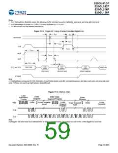
Figure 11.12 Data# Polling Timings (During Embedded Algorithms)
tRC
Addresses
CE#
VA
tACC
tCE
VA
VA
tCH
tOE
OE#
WE#
tOEH
tDF
tOH
High Z
DQ7
Valid Data
Complement
Complement
True
High Z
DQ6–DQ0
Status Data
True
Valid Data
Status Data
tBUSY
RY/BY#
Document Number: 002-00886 Rev. *B
Page 58 of 83

 INFINEON [ Infineon ]