S29GL01GP
S29GL512P
S29GL256P
S29GL128P
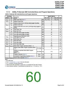
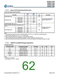
11.7.5
Erase And Programming Performance
Erase And Programming Performance
Typ
(Note 1)
Max
(Note 2)
Parameter
Unit
Comments
Sector Erase Time
0.5
64
3.5
256
sec
S29GL128P
Excludes 00h programming
prior to erasure (Note 4)
S29GL256P
S29GL512P
S29GL01GP
128
256
512
480
512
Chip Erase Time
sec
1024
2048
Total Write Buffer Time (Note 3)
µs
µs
Total Accelerated Write Buffer Programming Time
(Note 3)
432
Excludes system level
overhead (Note 5)
S29GL128P
123
246
492
984
S29GL256P
Chip Program Time
sec
S29GL512P
S29GL01GP
Notes
1. Typical program and erase times assume the following conditions: 25°C, 3.6 V VCC, 10,000 cycles, checkerboard pattern.
2. Under worst case conditions of -40°C, VCC = 3.0 V, 100,000 cycles.
3. Effective write buffer specification is based upon a 32-word write buffer operation.
4. In the pre-programming step of the Embedded Erase algorithm, all bits are programmed to 00h before erasure.
5. System-level overhead is the time required to execute the two- or four-bus-cycle sequence for the program command. See Tables –.
11.7.6
TSOP Pin and BGA Package Capacitance
Package Capacitance
Parameter Symbol
Parameter Description
Input Capacitance
Test Setup
VIN = 0
Typ
6
Max
10
Unit
pF
pF
pF
pF
pF
pF
CIN
COUT
Output Capacitance
Control Pin Capacitance
Separated Control Pin
Separated Control Pin
Separated Control Pin
VOUT = 0
VIN = 0
10
8
12
CIN2
10
WP#/ACC
RESET#
CE#
VIN = 0
42
25
22
45
VIN = 0
28
VIN = 0
25
Notes
1. Sampled, not 100% tested.
2. Test conditions TA = 25°C, f = 100 MHz.
Document Number: 002-00886 Rev. *B
Page 62 of 83

 INFINEON [ Infineon ]