S29GL01GP
S29GL512P
S29GL256P
S29GL128P
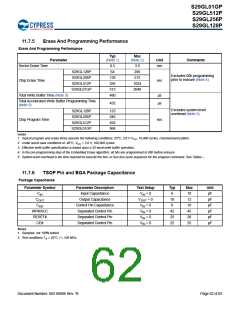
11.7.4
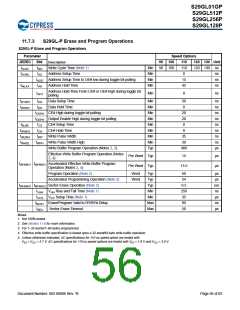
S29GL-P Alternate CE# Controlled Erase and Program Operations
S29GL-P Alternate CE# Controlled Erase and Program Operations
Parameter
Description
Speed Options
JEDEC
Std.
tWC
tAS
90 100
110
110
0
120 130 Unit
(Notes)
tAVAV
Write Cycle Time (Note 1)
Address Setup Time
Min 90 100
120 130 ns
tAVWL
Min
Min
Min
ns
ns
ns
tASO Address Setup Time to OE# low during toggle bit polling
15
45
tELAX
tAH
Address Hold Time
Address Hold Time From CE# or OE# high during toggle bit
polling
tAHT
Min
0
ns
tDVEH
tEHDX
tDS
tDH
Data Setup Time
Data Hold Time
Min
Min
Min
Min
30
0
ns
ns
ns
ns
tCEPH CE# High during toggle bit polling
tOEPH OE# High during toggle bit polling
20
20
Read Recovery Time Before Write
tGHEL
tGHEL
Min
0
ns
(OE# High to CE# Low)
tWLEL
tEHWH
tELEH
tEHEL
tWS
tWH
tCP
WE# Setup Time
WE# Hold Time
CE# Pulse Width
Min
Min
Min
Min
Typ
0
0
ns
ns
ns
ns
µs
35
30
480
tCPH CE# Pulse Width High
tWHWH1 tWHWH1 Write Buffer Program Operation (Notes 2, 3)
Effective Write Buffer Program Operation (Notes
2, 4)
Per Word Typ
15
µs
µs
Effective Accelerated Write Buffer Program
Operation
Per Word Typ
13.5
(Notes 2, 4)
Program Operation (Note 2)
Accelerated Programming Operation (Note 2)
tWHWH2 tWHWH2 Sector Erase Operation (Note 2)
Word
Word
Typ
Typ
Typ
60
54
µs
µs
0.5
sec
Notes
1. Not 100% tested.
2. See DC Characteristics on page 52 for more information.
3. For 1–32 words/1–64 bytes programmed.
4. Effective write buffer specification is based upon a 32-word/64-byte write buffer operation.
5. Unless otherwise indicated, AC specifications are tested with VIO = 1.8 V and VCC = 3.0 V.
Document Number: 002-00886 Rev. *B
Page 60 of 83

 INFINEON [ Infineon ]