IMW120R140M1H
CoolSiC™ 1200V SiC Trench MOSFET
Electrical Characteristics
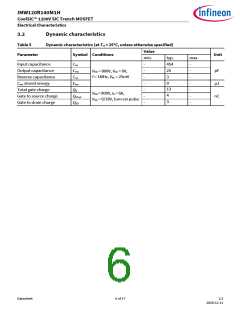
3.3
Switching characteristics
Table 6
Switching characteristics, Inductive load 4
Symbol Conditions
Parameter
Value
Unit
min.
typ.
max.
MOSFET Characteristics, Tvj = 25°C
Turn-on delay time
Rise time
td(on)
tr
td(off)
tf
VDD = 800V, ID = 6A,
VGS = 0/18V, RG,ext = 2Ω,
Lσ = 40nH,
diode:
body diode at VGS = 0V
see Fig. E
-
-
-
-
-
-
-
5
-
-
-
-
-
-
-
2.4
10.4
13
86
11
97
ns
µJ
Turn-off delay time
Fall time
Turn-on energy
Turn-off energy
Total switching energy
Eon
Eoff
Etot
Body Diode Characteristics, Tvj = 25°C
Diode reverse recovery
charge
Qrr
VDD = 800V, ISD = 6A,
VGS at diode = 0V,
dif/dt= 1000A/µs,
Qrr includes also QC ,
see Fig. C
nC
A
-
-
100
2
-
-
Diode peak reverse
recovery current
Irrm
MOSFET Characteristics, Tvj = 175°C
Turn-on delay time
Rise time
td(on)
tr
td(off)
tf
VDD = 800V, ID = 6A,
VGS = 0/18V, RG,ext = 2Ω,
Lσ = 40nH,
diode:
body diode at VGS = 0V
see Fig. E
-
-
-
-
-
-
-
5
-
-
-
-
-
-
-
5.8
10.4
13
ns
µJ
Turn-off delay time
Fall time
Turn-on energy
Turn-off energy
Total switching energy
Eon
Eoff
Etot
110
12
122
Body Diode Characteristics, Tvj = 175°C
Diode reverse recovery
charge
Qrr
VDD = 800V, ISD = 6A,
VGS at diode = 0V,
dif/dt= 1000A/µs,
Qrr includes also QC ,
see Fig. C
nC
A
-
-
125
3
-
-
Diode peak reverse
recovery current
Irrm
4 The chip technology was characterized up to 200 kV/µs. The measured dV/dt was limited by measurement test
setup and package.
Datasheet
7 of 17
2.2
2020-12-11

 INFINEON [ Infineon ]