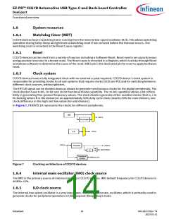
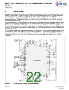
EZ-PD™ CCG7D Automotive USB Type-C and Buck-boost Controller
Dual-port
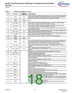
Pin list
Table 2
CCG7D pinout table (continued)
GPIO port
Pin#
Pin name
Description
assignment
GPIO. This GPIO is pulled-down during reset/power-up, as it is used to disable the FET
for the Vbat to GND short circuit protection for Port 0. Set the correct drive mode, if
the Vbat to GND short circuit protection is not required in the design.
20
GPIO2
P0.2
21
22
GPIO3
GPIO4
P0.3
P0.4
GPIO
USB D+ of Port 0 / GPIO: D+ for implementing BC 1.2, AFC, QC or Apple charging.
CCG7D does not support USB data transmission on this pin.
23
24
25
26
27
DP_0_GPIO5
DM_0_GPIO6
VDDD
P1.0
P1.1
–
USB D- of Port 0 / GPIO: D- for implementing BC 1.2, AFC, QC or Apple charging.
CCG7D does not support USB data transmission on this pin.
5-V LDO output. Connect a 1-µF ceramic bypass capacitor to this pin. Also, connect
this pin directly to pin 63.
USB D- of port 1/GPIO: D- for implementing BC 1.2, AFC, QC or Apple charging. CCG7D
does not support USB data transmission on this pin.
DM_1_GPIO7
DP_1_GPIO8
P1.2
P1.3
USB D+ of port 1/ GPIO: D+ for implementing BC 1.2, AFC, QC or Apple charging. CCG7D
does not support USB data transmission on this pin.
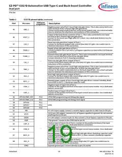
28
29
30
XRES
GPIO9
GPIO10
–
External reset – Active low. Contains a 3.5 KΩ to 8.5 KΩ internal pull-up.
P2.0
P2.1
GPIO
GPIO. This GPIO is pulled-down during reset/power-up, as it is used to disable the FET
for the Vbat to GND short circuit protection for Port 1. Set the correct drive mode, if
the Vbat to GND short circuit protection is not required in the design.
31
32
33
GPIO11
P1.4
P1.5
P1.6
GPIO / positive terminal of low-side current sense amplifier (LS CSA) of Port 1.
Connect to the positive terminal of the VBAT – GND short protection current sense
resistor.
CSP_1_GPIO12
CSN_1_GPIO13
GPIO / negative terminal of low-side CSA of Port 1.
Connect to the negative terminal of the VBAT – GND short protection current sense
resistor.
34
35
GND
Chip ground. Connect directly to the exposed pad (EPAD) and to pin 64.
VBUS NFET gate driver output of Port 1.
Connect to the provider NFET’s gate.
VBUS_CTRL_1
Type-C connector configuration channel 2 of Port 1.
Connect directly to the CC2 pin on the port’s Type-C connector. Also connect a 390-pF
capacitor to ground.
36
CC2_1
Type-C connector configuration channel 1 of Port 1.
Connect directly to the CC1 pin on the port’s Type-C connector. Also connect a 390-pF
capacitor to ground.
37
38
39
CC1_1
Type-C connector BUS voltage of Port 1.
VBUS_C_1
VBUS_IN_1
Connect to the Type-C connector’s VBUS pin.
Input of feedback voltage of error amplifier of Port 1.
Connect to the VBUS node between the output current sense resistor and the VBUS
provider NFET.
–
Negative input of output CSA of Port 1.
40
41
42
CSNO_1
CSPO_1
COMP_1
Connect to negative terminal of the output current sense resistor.
Positive input of output CSA of Port 1.
Connect to positive terminal of the output current sense resistor.
EA output pin of Port 1. Connect a compensation network to GND. Contact Infineon
for assistance in designing the compensation network.
Boosted power supply of Port 1 boost high side gate driver. Connect Schottky diode
from VDDD to BST2_1. Bootstrap capacitor node. Also, connect a bootstrap capacitor
from this pin to SW2_1.
43
44
BST2_1
HG2_1
Boost high side gate driver output of Port 1.
Connect to the boost (output) side sync (high side) FET gate. Use a wide trace to
minimize inductance of this connection.
Datasheet
18
002-28172 Rev. *N
2023-01-31

 INFINEON [ Infineon ]