EZ-PD™ CCG7D Automotive USB Type-C and Buck-boost Controller
Dual-port
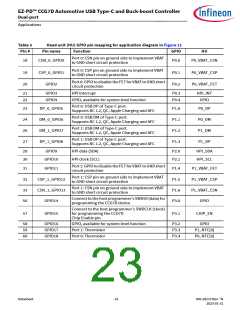
Pin list
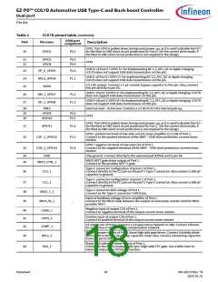
Table 2
CCG7D pinout table (continued)
GPIO port
Pin#
Pin name
Description
assignment
Negative power rail of Port 1 boost high side gate driver. This is also connected to one
input terminal of RCP of boost high side gate driver.
45
46
SW2_1
Connect to the switch node (inductor) on the boost (output) side. Use a short and wide
trace to minimize the inductance and resistance of this connection.
Output of the buck-boost converter of Port 1. This is also connected to one input
terminal of RCP of boost high side gate driver.
VOUT_1
Connect to the boost sync (high side) FET’s drain. Use a dedicated (Kelvin) trace for
this connection.
Boost low side gate driver output of Port 1.
47
48
49
50
LG2_1
PVDD_1
PGND_1
LG1_1
Connect to the boost (output) side control (low side) FET gate. Use a wide trace to
minimize inductance of this connection.
Supply of low side gate driver of Port 1.
Connect to VDDD. Use a 1 µF and 0.1 µF bypass capacitors as close to the CCG7D device
as possible.
Ground of low-side gate driver of port 1. This is also connected to one input terminal
of zero current detection of buck low side gate driver.
Connect directly to Port 0’s board ground plane.
–
Buck Low side gate driver output of Port 1.
Connect to the buck (input) side sync (low side) FET gate. Use a wide trace to minimize
inductance of this connection.
Negative power rail of Port 1 buck high side gate driver. This is also connected to one
input terminal of zero current detection of buck low side gate driver.
51
SW1_1
Connect to the switch node (inductor) on the buck (input) side. Use a short and wide
trace to minimize the inductance and resistance of this connection.
Buck high side gate driver output of Port 1.
52
53
54
HG1_1
BST1_1
CSNI_1
Connect to the buck (input) side control (high side) FET gate. Use a wide trace to
minimize inductance of this connection.
Boosted power supply of Port 1 buck high side gate driver. Connect Schottky diode
from VDDD to BST1_1. Bootstrap capacitor node.
Negative input of input CSA of Port 1.
Connect to the negative terminal of the input current sense resistor. Use a dedicated
(Kelvin) connection.
Positive input of input CSA of Port 1.
55
CSPI_1
Connect to the positive terminal of the input current sense resistor. Use a dedicated
(Kelvin) connection.
56
57
58
59
60
61
GPIO14/SWD_DAT
GPIO15/SWD_CLK
GPIO16
P3.0
P3.1
P3.2
P3.3
P3.4
GPIO/SWD programming and debug data signal
GPIO/SWD programming and debug clock signal
GPIO17
GPIO
GPIO18
VIN
4 V–24 V Input supply. Connect a ceramic bypass capacitor to GND close to this pin.
1.8-V core LDO output. Connect a 0.1-µF bypass capacitor to ground. Do not connect
anything else to this pin.
62
VCCD
63
64
VDDD
GND
5-V LDO output. Connect to pin 25. Also connect a 10-µF bypass capacitor to this pin.
Chip ground. Connect to the EPAD and to pin 34.
Positive input of input CSA of Port 0. Connect to the positive terminal of the input
current sense resistor. Use a dedicated (Kelvin) connection.
65
CSPI_0
Negative input of input CSA of Port 0.
–
66
CSNI_0
Connect to the negative terminal of the input current sense resistor. Use a dedicated
(Kelvin) connection.
Boosted power supply of Port 0 buck high side gate driver. Bootstrap capacitor node.
Connect Schottky diode from VDDD to BST1_0. Also, connect a bootstrap capacitor
from this pin to SW1_0.
67
68
BST1_0
Buck high side gate driver output of Port 0.
HG1_0
EPAD
Connect to the buck (input) side control (high side) FET gate. Use a wide trace to
minimize inductance of this connection.
Exposed ground pad. Connect directly to pins 34 and 64.
Datasheet
19
002-28172 Rev. *N
2023-01-31

 INFINEON [ Infineon ]